Blogpost PCB requirement (L1-11)

Written by: Forrest Pino

Edited and Approved by: Carolina Barrera

Table of Contents

Intro:

In order to fulfill the L1-11 system requirement “Custom PCB” an analysis has been carried out. This test followed the Verification and Validation Test Plan. This requirement was one that applied to all the groups in EE 400D. It requires that groups develop a custom PCB that help the network and controller communication in the electronic system of the project.


Test Objective:

The test criteria that needs to be tested are provided by Prof. Hill in this class document[1]:

Prof. Hill provided multiple criteria which the Custom PCB should follow, and set a grade scale accordingly. For this project an “A”-Grade was desired.

Therefore this criteria apply:


“All components (resistors, capacitors, LEDs, IC chips) are surface mount. Some exceptions are header pins and large electrolytic capacitors, and components not available in surface mount. All PCB traces were manually routed. Used only one surface mount IC component for the PCB design. All other non-IC components were surface mount (resistors, capacitors. LEDs, IC chips). All PCB traces were manually routed.”[2]

Equipment


  • Eagle Schematic and Layout
  • Soldered Custom PCB


The PCB schematic and layout were designed using Eagle. Most of the ICs were ordered through Digi-Key. They are all surface mount components. Upon arrival of the PCB and the ICs, the components were tested to make sure there were no shorts or burnt components. Manufacturing solder the board by hand the first version of our PCB, but voltage outputs from the buck converter were not right. Chances are the board got burnt or one of the pins of the IC3 was not solder properly.

As a solution, Electronics and Control purchased a stencil, and the second version of the PCB worked perfectly. However, there was one feature that could not be implemented; the kill-switch. The incident is explained fully in the corresponding blog post, but the safety feature was removed from the system.

Conclusion:

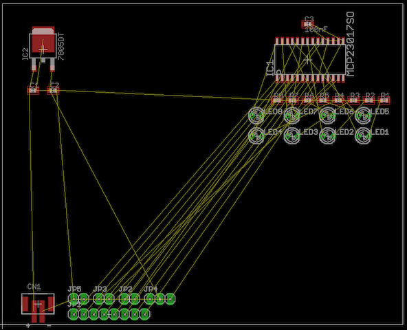
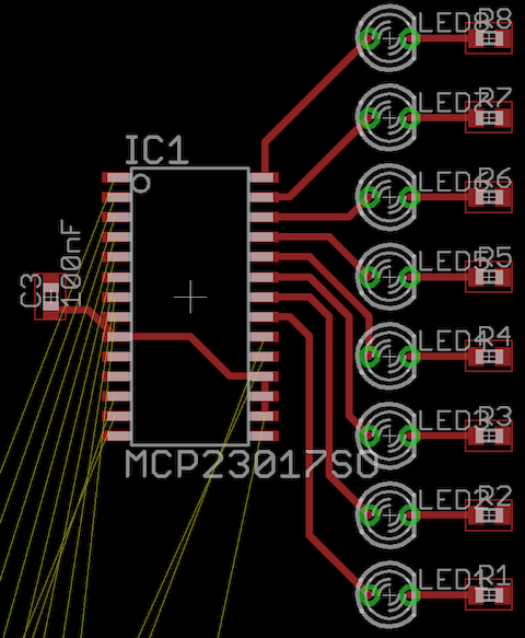
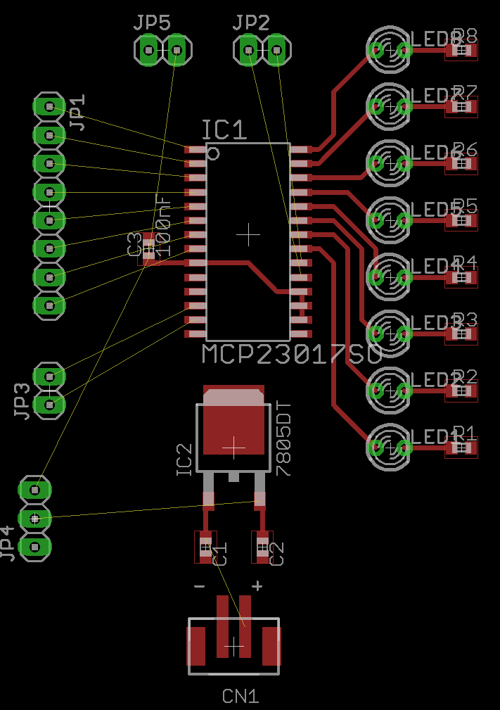
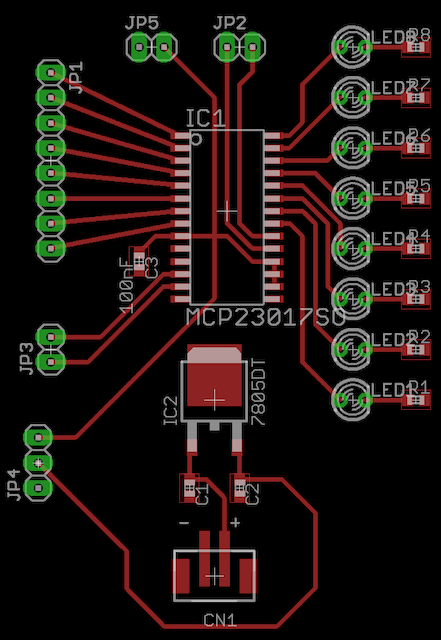
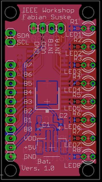
(Custom PCB) Showing all SMD components

On the Custom PCB are 2 Surface mount IC’s the Linear Technelogie LT3971-5 Buck Converter

(Showing the package of the Buck Converter)

as well as the Allegro A4988 stepper motor driver. The Buck is a DFN-10 Package. The motor driver is a QFN-28 package.


Both packages are a challenge to solder due to their small size.

The resistors and capacitors are all 0603. The Diode (DO-214AC) and the Inductor (1812) are bigger due to their availability.

Even the LDO is a Surface Mount Device. But this component is no challenge due to it’s big size (TO-263).

The connectors were implemented as PTH (Through hole) components.

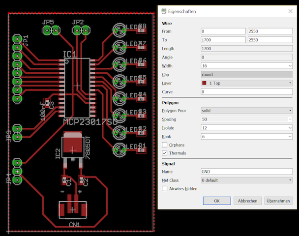
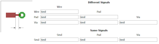
The traces were all manually routed following this instructions[3]

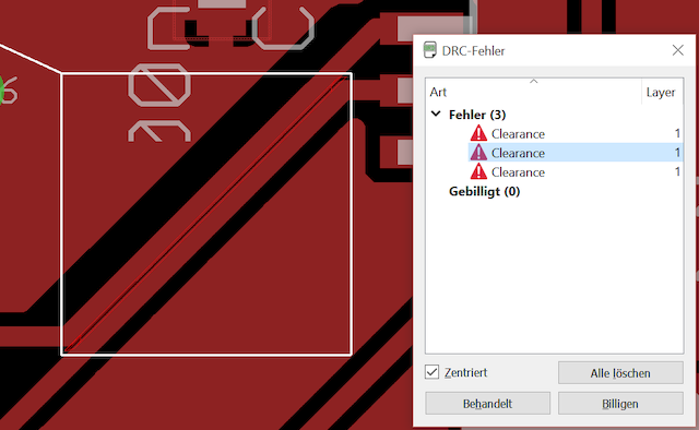
Afterwards the PCB was checked using a whole suit of DRC including OSH, Sparkfun and LeanPCB. The PCB passes every single one. Therefore the PCB passes this Analysis.

References

[1]http://web.csulb.edu/~hill/ee400d/Lectures/Week%2009%20Design%20Verification%20and%20Validation/a_Meeting%209%20Agenda%20F’16.pdf

[2]http://web.csulb.edu/~hill/ee400d/Lectures/Week%2009%20Design%20Verification%20and%20Validation/a_Meeting%209%20Agenda%20F’16.pdf

[3] http://arxterra.com/printed-circuit-board-pcb-how-to-layout/

MyoWare – MYOELECTRIC SENSOR

Written by: Carolina Barrera

Our muscles are controlled, and usually move thanks to electric impulses that produce contraction in these, and the reaction to that contraction is what we know as a movement. Electromyography technology was developed to evaluate and record this electrical activity.

Myoelectric signals are becoming popular in medicine and prosthetic technology probably because they are the most recent, and more practical control for people that are missing a limb. The great thing about this idea is that people left with the remaining of their limb can control the device. In other words, the technology is minimizing the difference of what could be consider a full-functional amputee and a full-functional non-amputee.

For our project, we are implementing an EMG sensor which sends an analog signal our MCU. A threshold voltage was set so when the voltage generated by the bicep goes over this value for a certain amount of time the motor is activated.  Since we need to move the arm up and down intervals were assigned. The longer interval will make the arm move down, and the short interval will make it move up.

To test the feasibility of implementing this type of control for our project we needed to see the different values the sensor outputs in the different patterns of motion in the arm (bicep and forearm).

We were not sure if flexing or tensioning the arm were more effective for achieving our threshold, and we wanted to make sure that one wouldn’t interrupt the movement of the other unintended. Our test shows the output of the sensor in four different patterns of moving and tensioning the bicep.

Luis wore the EMG sensor, and we use the built-in Serial sample from the Arduino IDE to read the analog values from the EMG.

We performed different motions with the arm to see which could get a stable high-signal for long enough, and also that I couldn’t be interrupted easily by other unintentional movements when lifting the arm.


Figure 1 shows four different actions that show significantly different outputs that could be implemented in the code when programming the sensor. The four action in chronological order are: relaxed arm, tensioned arm, lifted arm, and tensioned and lifted arm.

From the test, we concluded that tensioning and lifting the arm outputs a relatively large signal (compared to the other motions), and the signal is stable as long as we can keep the arm lifted and tensioned. Later on we discovered that twisting the arm also helps outputs a high signal, so in case up-and-down-movement is restricted we can always try twisting the arm.

We also discovered that the best location to position the sensor (with the electrodes) in the inner side of the bicep -by the side of the arm tha touches the torso. Figure 2 shows the position we put the sensor in the arm. As for the two electrodes, Sparkfun reccommends to place the sensor so one of the electrodes

Interface Integration Piece

Blog Post – Integration Interface

Written by: Carolina Barrera


As mentioned multiple times in our documents, we scheduled integration for the arm for November 19th. No physical integration happened on this day. We didn’t assemble the two systems together, however we made some advancements in the process of integrating the components together.

An idea the two groups wanted to achieved initially, in which our system has a uniform forearm connected the bicep to the hand, and helps harmonize the appearance of the overall system was very desired. It seemed more promising for obtaining a better result in the validation for both teams, and it could lessen the weight that extra pieces (in the integration) add to the system.

Based on this approach, there were a couple of ideas that were considered before bringing up this idea:

  1. The dimensions for the wrist height and width are 3 in. by 3 in, respectively. Adding a cover would mean that our wrist would have a dimension of 3.5 inches at least.
  2. The weight of connector parts, and big screws in-between subsystems would be minimized if we tried.
  3. A harmonized structure would give more opportunities to both groups to increase points in their validation grade.

In November 19th, the idea of a one-solid piece helping as a shell mechanism, and unedifying both the forearm and the arm was brought up to consideration. The ideas described above served as reasons for implementing this instead of having the two independent components, as agreed originally. We measured the parts that we have at the moment, and figure the rough length of this new piece. Figure 1 is a picture we took on that day that could help as reference of the dimensions of this new part, and the functionality it would have.

Figure 1 - Agreement Guideline Created on Nov. 19

Figure 1 – Agreement Guideline Created on Nov. 19

To achieve this, the department of design offered their help, and the Junior TA, Van Lieu shepherd both Manufacturing Engineers in finding an aesthetic way to integrate their pieces. The resulting design is shown in figure 2.


In regards to the agreement, there are items that were communicated as clarifications:

  1. The hand and the arm agreed in the idea of implementing a solid interface for integration. This “integration part” that serves as a shell is result of the design and manufacturing efforts of both Manufacturing Engineers, Forrest Pino and Wilson Mach under guidance of Van Lieu, Industrial Design student from CSULB.
  2. This part will house the motor for the hand that allows the wrist rotation on the hand side. Additionally, it will house the wires going to the PCB of the hand -located near to the “elbow”, and a slipring -that will prevent over-twisting and ripping of the wires when the wrist rotates.

We moved forward in the process of integration -even though we were not physically putting together the components. This meeting could be considered the initial phase of the integration, in which the baseline is set, and both groups agreed in dimensions, and restrictions that will direct our project into mission success. More updates will be posted if relevant changes come up in the project. However, with the time left, and the advance stage of both projects don’t give space to last-minute changes.


Printed Circuit Board (PCB) – How to Layout?

Table of Contents

Basics:

  • Only 45° angles
  • ICs on the 50 mil grid
  • At least 10 mil for signals
  • At least 16 mil for power
  • Add power planes (GND/GND or VDD/GND)

Steps in laying out a PCB:

Written by: Fabian Suske

Approved by: Carolina Barrera

0.      Checking the Schematics for Errors

You should get a working Schematic but mistakes happen. As an EE you should be able to understand Schematics and know what’s going on. There you should check for silly mistakes like missing Power (GND/VDD) decoupling capacitors or any project related errors (missing /to many parts). If you want to be extra sure pull up the datasheet and check if the typical application is followed. (Capacitors on a voltage regulator) Make sure the ERC has no errors.

1.      Sort the components

Take your schematics and identify groups of components. Take every IC and spread them out.  Now take all the small components (Resistors, Capacitors, etc.) and place them as close to the IC pins as possible. Make sure they’re on the correct pins. (I.E. decoupling pins close to VDD pin not GND pin).

Make sure all the connectors and small stuff (power LEDs with resistors) are out of the way. You don’t need them yet.

1_k

2.      Connect the components.

The first thing you do is locate one ground wire and in the properties hide air wires. We will add at least one GND plane later.

On your separate groups try to connect all air wires with the least amount of space needed. (Make sure you used ratsnest before you start routing). At this point the amount of vias should be very low. Don’t spend too much time finding the ideal route – route the traces fast (you most likely rip them up again anyway). If you have a rather compact setup for each group.

SMD Pads should be connected from directly in front or behind.

Also keep the trace with in width in mind. Like you wouldn’t run 10A through 35 gauge wire. A drawn wire can only handle a certain amount of current. http://www.4pcb.com/trace-width-calculator.html

2_k   figure14 3_k

Note the wrong connection on LED 8 (top one) and the overlap on C3. Fix them now!!

3.      Moving the groups into position

After you briefly routed the groups it’s important to move the groups into their “final” position. Therefore take the main IC or MCU and place it in the middle. Now move the groups somewhere close to the MCU. You should bear in mind that connectors might needs to be connected (so plane your space). You might want to mirror the group to utilize the space efficiently. Most likely you have some overlapping components or vias in the way. Rip them up and reroute them. Connect the air wires between the ICs at this time to (as well as to the MCU).

4


4.      Placing the rest of the components

Now you should place the connectors into a logical space. This is different for each project. Typically it makes no sense to place a connector on the other end of the chassis /PCB. You should have cable management in mind. You also should place them as close as possible to the IC’s

Fill in the gaps with less important stuff like power LEDs or optional headers.

If your done move everything to the origin and adjust the board dimensions

Note non 45° degrees on JP1. 90° in the middle are okay since more than one trace.

5_k

5.      Power Planes

Normally on a dual layer PCB you have two GND planes (referred to GND-GND). On small PCBs you might want to have a VDD plane as well (VDD-GND). Apply were applicable.

To add a Power plane you take the polygon tool and completely enclose your PCB. Click then on the name tool and give it the name of your power signal (GND, VDD +3V3 or +5V or whatever). Then open the properties for them and change the rank to 6 and isolate to 12. Also uncheck the “hide air wires” now.

You might see some un-routed air wires now. Connect them to the respective power plane. In order to achieve this you might want to move some components or wires in order to make space for the power plane to reach this plank spots. Adding a via might help as well.

If you have two GND planes you should add some vias in big blanc spots.

6_k

7_k

To resolve this air wire we add a GND Via

6.      DRC

If all air wires are connected (An easy way to check is to deselect all layers except of dimension and Unrouted). Click the Design Rule Check (DRC). Before running the DRC go to clearance and change every value to 6mil. Also change Limit under Mask to 50. (This will give you tented vias (looks nicer))

Then hid apply and run. Fix all issues like overlap, clearance etc. (If you added a via on an IC ground pad you may approve it.).

8_k

9_k

10_k

7.      Tweaks, Labels and Holes

The last step after fixing the errors involves making tweaks to the PCB. You might want to reduce the size or fix funny routing (non necessary bends). Also make sure all component names are visible. In order to move them you need to smash the component this will add an origin “+” to the name and you can move them now. Make sure that no name is over a component or pad. If you have tented vias you can place them above vias.

Last but not least you need to add individual text (on the tPlace or bPlace layer) and label all connectors with their respective signals like SDA and SCL for I2C.

If you might have space you can add a project name or maybe even the members name on the PCB.

If you moved wires or vias or even components in order to place Text nice, you need to rerun the DRC each time you messed with the layout.

You might also want to add mounting holes to the PCB here make sure you have enough room for the screw caps.

11_k

Note that I changed the design completely to make it way smaller

Integrated Control Document

Written by: Luis Martinez

Approved by: Carolina Barrera

The purpose of the Integrated Control Document (ICD) between the Prosthetic Arm and Prosthetic Hand systems, as an integrated Upper-Limb Prosthetic System, is to capture essential categories of interaction between both systems upon their unification. This document details explicit responsibilities and agreements between each of the respective groups, and serves as an approved reference document for both project groups to refer to, as a standard for design objectives shared amongst both groups.

Of key regard amongst shared transactions between both groups are those for power, attachment, mass, size, and volume accommodation. Below is a high-level description of these categories:

Power – The Prosthetic Arm will supply power to the Prosthetic Hand via 3x, 22 AWG cables (12V, 5V, GND), allowing up to 3500 mA on 12V, and 1000 mA on 5V from a 1600-mAh, 14.8-V Lithium-Ion Polymer (LiPo) battery stored in the bicep of the Prosthetic Arm system.

Attachment – The Prosthetic Hand will be responsible for allocation of the wrist, of dimensions 76.2 mm x 76.2 mm ± 12.7 mm (3 in x 3 in ± 0.5 in margin). The mounting interface between both systems will be a squared, plated-screw type consisting of 4x, 4-mm screws and a hollow center, allowing the Prosthetic Arm to feed power cables to the Prosthetic Hand in such a way that they are not operationally inhibited by the rotation of the wrist. Furthermore, the Prosthetic Hand will be responsible for any cabling related to storage of their micro-controller (MCU) and printed circuit board (PCB) components within the Prosthetic Arm portion of the integrated system.

Mass – The forearm, hand, and food sustained by the Upper-Limb Prosthetic System should not exceed a combined weight of 6.83 lbs. to correspond with a torque of 10.634 NM at 35 cm for the stepper motor localized at the elbow by the Prosthetic Arm. From this, the Prosthetic Hand will have an allocation of 1.35 ± 0.23 kg (2.97 ± 0.5 lbs.), with an expected weight for the heaviest food item (21 fl oz. drink) at 0.69 kg (1.52 lb.). Overall, the system should be no heavier than 4.0 ± 0.61 kg (8.82 ± 1.35 lbs.).

Size – The Prosthetic Arm, in conjunction with the Prosthetic Hand should be no longer than 35 cm ± 5 cm (13.78 in ± 1.55 in) from elbow to tip of middle finger, from which the Prosthetic Hand will measure 269 ± 13 mm (10.6 in ± 0.51 in) from end of wrist/ forearm attachment to tip of middle finger.

Accommodation (Volume) – As referenced above, the Prosthetic Arm will provide space accommodations for the MCU, PCB units of the Prosthetic Hand, of dimensions 83 mm x 64 mm x 38 mm (3.25 in x 2.5 in x 1.5 in) in effort to alleviate space constraints faced by the Prosthetic Hand.

After the Preliminary Design Review (PDR), suggestions from the customer and class presidents were taken into consideration by both groups, and agreements were reached with respect to the following new categories:

  • Noise: Prosthetic Arm, in conjunction with Prosthetic Hand, will not exceed 60 dB during operation.
  • Safety: Prosthetic Arm will implement an electronic kill switch to disconnect the power supply to the Prosthetic Hand and the Upper-Limb Prosthetic System in the case of a perceived emergency situation or safety concern.
  • Schedule: Prosthetic Arm and Prosthetic Hand groups will have their respective systems ready for integration by an agreed-upon tentative date of Saturday, 11/19/16
  • Aesthetics: Prosthetic Arm, in conjunction with Prosthetic Hand, will have a matching outer appearance, such that in the case of wearing a sleeve and glove respectively, the Upper-Limb Prosthetic System will not attract unwarranted attention.
icd_2

Prosthetic Arm Overview

Moving forward, certain category estimates will be refined, such as the estimated noise threshold to correlate with experimental studies from a McDonalds site visit, and an integrated temperature sensor in the circuitry of the Prosthetic Arm that will be programmed to detect significant deviations from the operating temperature of the Upper-Limb Prosthetic System once integration has been achieved.

Furthermore, an option to vacuu-form, in terms of aesthetics, is being explored by the Prosthetic Arm system in collaboration with the CSULB Design Department pertaining to guidance and permission to use related facilities and equipment. Further changes to this approved document will be submitted for approval, and captured as supplemental revisions.

Prosthetic System Definition Update

After testing the EMG sensor and a joint meeting with the Hand group, the responsibilities of each E&C division had been set in stone. The decisions of this meeting had been protocolled in meeting minutes as well as on a drawing with each member signed.

fabians1

Figure 1 – E&C Agreement with the Hand

In the following weeks the Level 1 and Level 2 requirements had been finalized and the System Block Diagram could be updated. In the final design two indicator LEDs had been added as well as a Kill Switch. The Kill Switch gives the user the possibility to power off the system (immediately) in the event he doesn’t feel comfortable with the systems behavior.

Also there’s no need to communicate between the two systems anymore so the I2C lines had been removed.

The tests of the MyoWare muscle sensor also came to the conclusion that one motion can be tracked sufficient enough with one sensor. But a second sensor is not enough to provide a second motion. A second motion might be accomplished with a third sensor. Since the Project requirement can be fulfilled with one motion and in regard to the budget only one EMG sensor will be used.

All this led to this updated System Block Diagram.

Figure 2 - Resulting and Updated Block System Diagram

Figure 2 – Resulting and Updated Block System Diagram