Fall 2016 Biped – Arexterra Control Panel

Table of Contents

Control Panel

By: Brandon Perez (Missions, Systems, and Test Engineer)
Approved by: Ijya Karki (Project Manager)

Introduction

The predefined move command in Arxterra Control Panel located at address 0x01 operates under parameters set by the Directional Buttons (D-PAD) widget which is already on the control panel by default.

Panel Image

control-panel

Discussion

How we will use these data packet values to our advantage?

Since our MCU receives [A5 N 01 01 X 01 X LRC]. If the data transmission is successful, then we are only concerned with the highlighted values in the data packet [A5 N 01 01 X 01 X LRC]. The first value in the highlighted part of the data packet is the address of the predefined or custom command. In the data packet, 01 01 X 01 X, the green highlighted part of the code “01” is the command address. The following blue highlighted part of the data packet, “01 X 01 X”, are the parameters. Our goal to operate our Biped is to utilize these parameters to effectively have our Biped walk forward, turn left, and turn right. We will have to modify the code in the move command to include control of servos to have our Biped turn and walk without the use of any custom commands.

Printed Circuit Board (PCB) – How to Layout?

Table of Contents

Basics:

  • Only 45° angles
  • ICs on the 50 mil grid
  • At least 10 mil for signals
  • At least 16 mil for power
  • Add power planes (GND/GND or VDD/GND)

Steps in laying out a PCB:

Written by: Fabian Suske

Approved by: Carolina Barrera

0.      Checking the Schematics for Errors

You should get a working Schematic but mistakes happen. As an EE you should be able to understand Schematics and know what’s going on. There you should check for silly mistakes like missing Power (GND/VDD) decoupling capacitors or any project related errors (missing /to many parts). If you want to be extra sure pull up the datasheet and check if the typical application is followed. (Capacitors on a voltage regulator) Make sure the ERC has no errors.

1.      Sort the components

Take your schematics and identify groups of components. Take every IC and spread them out.  Now take all the small components (Resistors, Capacitors, etc.) and place them as close to the IC pins as possible. Make sure they’re on the correct pins. (I.E. decoupling pins close to VDD pin not GND pin).

Make sure all the connectors and small stuff (power LEDs with resistors) are out of the way. You don’t need them yet.

1_k

2.      Connect the components.

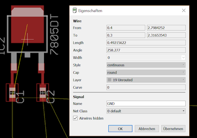
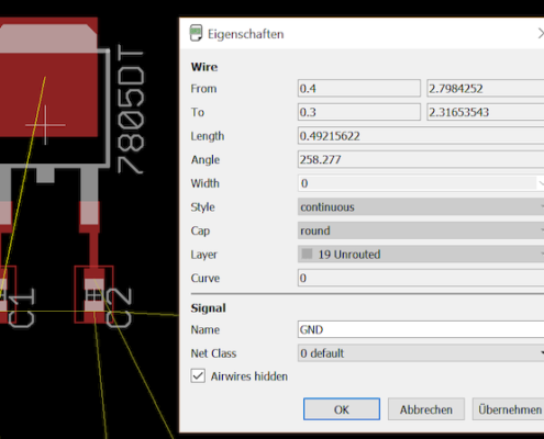
The first thing you do is locate one ground wire and in the properties hide air wires. We will add at least one GND plane later.

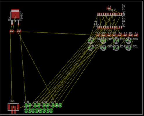
On your separate groups try to connect all air wires with the least amount of space needed. (Make sure you used ratsnest before you start routing). At this point the amount of vias should be very low. Don’t spend too much time finding the ideal route – route the traces fast (you most likely rip them up again anyway). If you have a rather compact setup for each group.

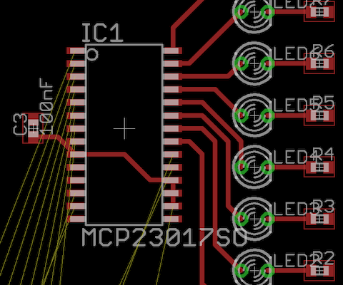
SMD Pads should be connected from directly in front or behind.

Also keep the trace with in width in mind. Like you wouldn’t run 10A through 35 gauge wire. A drawn wire can only handle a certain amount of current. http://www.4pcb.com/trace-width-calculator.html

2_k   figure14 3_k

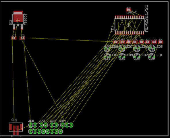
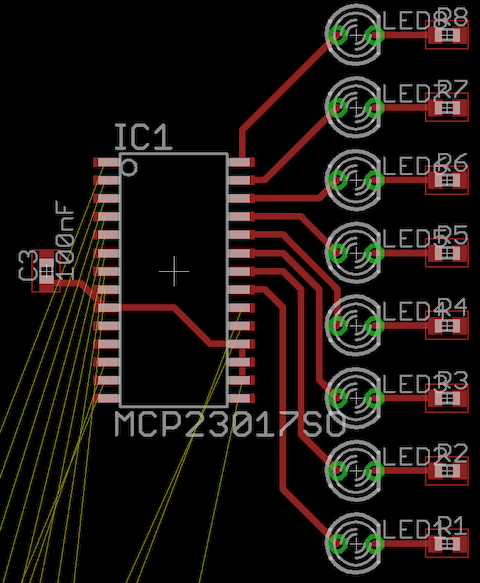
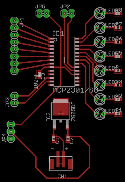
Note the wrong connection on LED 8 (top one) and the overlap on C3. Fix them now!!

3.      Moving the groups into position

After you briefly routed the groups it’s important to move the groups into their “final” position. Therefore take the main IC or MCU and place it in the middle. Now move the groups somewhere close to the MCU. You should bear in mind that connectors might needs to be connected (so plane your space). You might want to mirror the group to utilize the space efficiently. Most likely you have some overlapping components or vias in the way. Rip them up and reroute them. Connect the air wires between the ICs at this time to (as well as to the MCU).

4


4.      Placing the rest of the components

Now you should place the connectors into a logical space. This is different for each project. Typically it makes no sense to place a connector on the other end of the chassis /PCB. You should have cable management in mind. You also should place them as close as possible to the IC’s

Fill in the gaps with less important stuff like power LEDs or optional headers.

If your done move everything to the origin and adjust the board dimensions

Note non 45° degrees on JP1. 90° in the middle are okay since more than one trace.

5_k

5.      Power Planes

Normally on a dual layer PCB you have two GND planes (referred to GND-GND). On small PCBs you might want to have a VDD plane as well (VDD-GND). Apply were applicable.

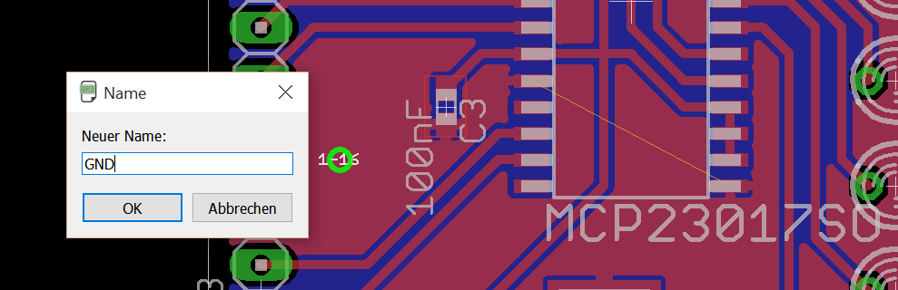
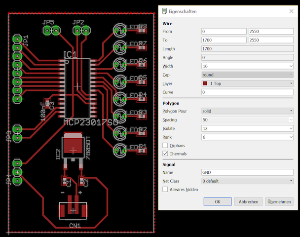
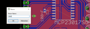
To add a Power plane you take the polygon tool and completely enclose your PCB. Click then on the name tool and give it the name of your power signal (GND, VDD +3V3 or +5V or whatever). Then open the properties for them and change the rank to 6 and isolate to 12. Also uncheck the “hide air wires” now.

You might see some un-routed air wires now. Connect them to the respective power plane. In order to achieve this you might want to move some components or wires in order to make space for the power plane to reach this plank spots. Adding a via might help as well.

If you have two GND planes you should add some vias in big blanc spots.

6_k

7_k

To resolve this air wire we add a GND Via
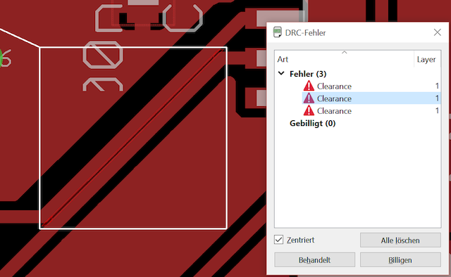
6.      DRC

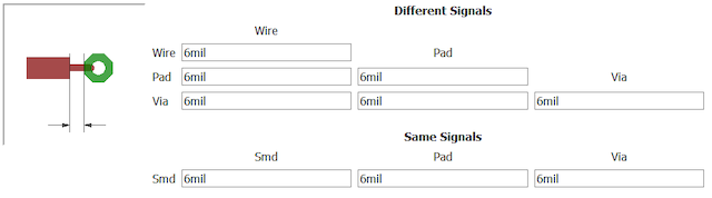
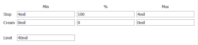
If all air wires are connected (An easy way to check is to deselect all layers except of dimension and Unrouted). Click the Design Rule Check (DRC). Before running the DRC go to clearance and change every value to 6mil. Also change Limit under Mask to 50. (This will give you tented vias (looks nicer))

Then hid apply and run. Fix all issues like overlap, clearance etc. (If you added a via on an IC ground pad you may approve it.).

8_k

9_k

10_k

7.      Tweaks, Labels and Holes

The last step after fixing the errors involves making tweaks to the PCB. You might want to reduce the size or fix funny routing (non necessary bends). Also make sure all component names are visible. In order to move them you need to smash the component this will add an origin “+” to the name and you can move them now. Make sure that no name is over a component or pad. If you have tented vias you can place them above vias.

Last but not least you need to add individual text (on the tPlace or bPlace layer) and label all connectors with their respective signals like SDA and SCL for I2C.

If you might have space you can add a project name or maybe even the members name on the PCB.

If you moved wires or vias or even components in order to place Text nice, you need to rerun the DRC each time you messed with the layout.

You might also want to add mounting holes to the PCB here make sure you have enough room for the screw caps.

11_k

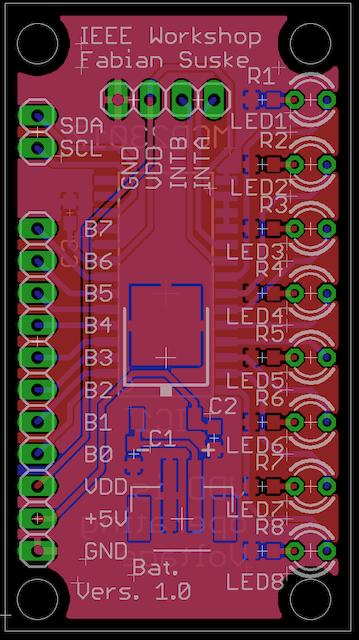
Note that I changed the design completely to make it way smaller

Fall 2016 Solar Panels: I2C Communication Experiment

By Jose Rodriguez (Electronics & Control)

Approved By Inna Echual (Project Manager)

Objective: Currently, we will be using our own Arduino Leonardo while the Thursday Pathfinder group (referred to as the chassis group) will also have their own Arduino Leonardo. The solar panels Arduino and chassis Arduino will communicate using I2C interface on Arduino. In order to ensure the concept is understood completely, the following experiment was done with an Arduino Mega and Arduino Uno, where the Mega was used as the Master and the Uno as the slave.

The following were the components used for the experiment:

  • Arduino Uno
  • Arduino Mega
  • LED
  • Resistor
  • Breadboard

untitled1

Figure 1: Code to set up Mega as master

The code in Figure 1 was used to set up the Arduino Mega as the master. The serial monitor was used to debug the system; however it can be removed without affecting the code. Wire.Begin starts the communication using the I2C and address must be inputted. Wire, write is then used to send data to the Arduino. To end the communication using the I2C, Wire.endtransmission needs to be used.

 untitled3

Figure 2: Code to set up Uno as slave


The code in Figure 2  was used to set the Arduino Uno as the slave. The key difference is that the Arduino is given an address by writing wire.begin followed with address. The address given to the Arduino is 400 because of the class but any number could have been used. In addition, a subroutine has to be made so that when data is sent, the Arduino goes to the function and does something with the data received. Note that the function called cocoon was created but any other function can be used.

Figure 3 shows the Fritzing Diagram showing how the circuit is configured.

untitled4

Figure 3: Fritzing Diagram

untitled5

Figure 4: Visual Results of Experiment

Figure 4 shows the results of our experiment, i.e. our code working: every time the button is pressed, the Arduino Mega reads the value and sends the value to the Arduino Uno. As a result, pin 13 is set to high whenever the value received is one. Since we do not have both projects done yet, I am using the button as the Arxterra signal that will tell Arduino mega to cocoon. A LED on means subroutine cocoon is active in the Arduino Uno and inactive if the LED is off.

This experiment verifies that communication between two Arduinos is possible.


Current Sensors Experiment

Current Sensing Experiment:

Purpose:

Measuring motor draw current on current sensing pins via the VNH5019 to identify no load conditions and determine no-load threshold to shut off motors.

The VNH5019 provides two current pins to the user, which can be used to measure the instantaneous current absorption by each H-Bridge.

Procedure:

While running a motor through the VNH5019, the current was measured using the Arduino Leonardo via the current sensing pins M1CS and M2CS. Through software, a running average smoothing filter was used to remove inconsistencies in the data. After graphing the current data drawn by the averagre, a threshold was determined. An ammeter was attached to the motor to directly compare the current measured with the Arduino data.

Results:

After reading the current measured by the Arduino, a current range was determined at which the motor ran under no load conditions. From the data, it was determined that under no load conditions, the current draw was between 450 mA and 600 mA. Using the Ammeter as a reference, it was found that the actual current draw of the motor was about 620 mA. The threshold for the current under no load conditions was chosen to be 620 mA.

picture3

Digital Slip Differential Voltage Ratio

By: Jose Alcantar, Electronics and Controls Engineer

Speed Ratio Calculation for slip differential

Purpose:

To implement slip differential turning, the speed ratio for the left and right set of wheels needs to be calculated. Further testing needs to be done to find a comfortable speed for the left and right wheels.

Procedure:

To determine the speed ratio, the distance each wheel travels was calculated. This ratio can then be applied to both the speed and the voltage applied to the motors,

R*θ is a way of working out how far a wheel travels on a circular path. An arc with 180° gives you a θ of π radians. For example, an arc with a radius of 40 inches, the total distance the pathfinder will travel on that arc is π * 40, or roughly 125 inches. But if the center of the pathfinder is on the arc, then each wheel will travel a different arc – one outside, one inside. The wheels on the pathfinder are about 18 inches apart, so each wheel is 9 inches from the center. One wheel is on an arc of 31 inches’ radius and the other is on an arc of 49 inches (40 +/- 9). The inside wheel will travel about 97 inches and the outside wheel will travel 153 inches. The ratio between the two distance will be 150:100 (rounding), or 1: 0.67, will always give you that arc. Regardless of speed if one wheel moves 1 inch at the same time the other moves 0.67 inches. Using this ratio, the arc will be given at any speed or voltage applied to the wheels.

picture2