Soldering Workshop
By: Diane Kim (Division Manager for E&C)
Verified By: Jordan Smallwood (Project Manager)
Approved By: Miguel Garcia (Quality Assurance)
Table of Contents
Introduction
The Soldering workshop was focused on hand soldering. Based on the PCB designs of each project, the components that were to be hand soldered were the through-hole components, more specifically the connectors and the IR LEDs. Since we had access to a soldering iron, we practiced soldering based on the guide from Adafruit to understand how to solder. I have access to a PCB fabricating machine called the Othermill from Batam tools and printed out practice circuits for the group to practice on as well as provide connectors if needed.
Guide To Soldering
Required Tools
- Solder Iron
- Wet Sponge/Brass Mess
- Solder
- Wires
- Through-Hole Components
- Solder Sucker/Wick
First Step: Check Tools/Materials
Before you turn on the soldering iron, make sure to check whether the tip is clean or not. If the tip is not clean (when it is oxidized) it can prevent the tip of the soldering iron from heating up properly. To make sure that this doesn’t happen, we need to always make sure to clean the tip using the wet sponge and brass mesh and thin the tip after each use so the tip acts as a protective layer.
The type of solder also determines what temperature to set the iron on. If the solder is lead-based the temperature of the iron should be set to around 650 degrees Fahrenheit, and if the solder is lead-free it is best to set the temperature around 750 degrees Fahrenheit. The temperature setting is important to properly heat up the conductive pads and the wires or through-hole components.
Soldering
When the soldering iron reaches the desired temperature, the iron is placed in the joint of the pad and the component wire lead. The solder should first touch the iron and then to the wire lead and the pad for a secure connection. Then remove the iron and solder for it to cool. It is also important to make sure that the heat is not applied for too long to prevent overheating. A good solder is when the solder covers the whole pad and the wire lead and it has a slanted slope connecting the wire lead and the pad. It also looks smooth and shiny on the surface. If the solder is dark and is in a ball like shape that means that not enough heat or uneven heat was applied to the pads which are called the cold joint.
Making Mistakes:
Sometimes when the pads are so close, it can be shorted during the soldering process. To remove the excess solder, you can use a solder sucker or solder wick to remove the solder. The solder sucker sucks the solder out and the solder wick soaks up the excess solder.
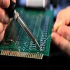
Soldering Workshop:
The groups first went over the basics of soldering and then I provided practice boards so that they could practice. The practice board consisted of connectors that varied in the number of pinheads (8, 6, 4, 3). Female connectors were also provided to practice soldering.
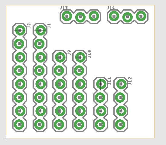
Figure 1: Eagle Board file of the practice board for soldering
The practice board consists of 2 of each 8, 6, 4, and 3 pinhead connectors.
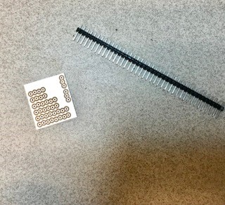
Figure 2: Photo of the practice board after printing and female connectors that are provided
Conclusion:
The group knew how to solder prior to the workshop but were able to practice to avoid making mistakes that would cost them the whole board. Since they were able to practice soldering on connectors which is what they will be soldering on for their PCB, it was more applicable to their projects.
When it comes to surface mount soldering, I went over the theory of how to apply the solder paste and how to bake the board; however, since I have access to a PCB fabrication machine that can print the solder paste and bake the board, we will be using that for the PCBs for our projects. The PCB fabrication machine that we are using is the V-one from Voltera.
References:
The information about soldering is based off a tutorial on Adafruit:
Fritzing Diagram Training
By: Diane Kim (Division Manager of E&C Hardware)
Verified By: Jordan Smallwood (Pathfinder Project Manager)
Approved by: Miguel Garcia (Quality Assurance)
Table of Contents
Introduction
Fritzing is a program that allows easy PCB design. It allows the user to convert their design on breadboard to CAD files. On the breadboard view, there are parts that are commonly used such as Arduino boards, resistors, motor drivers, and Bluetooth modules. The breadboard view can also be converted into the schematic.
Training
We spent one week on the training for the Fritzing program. We used the documentation from the EE400D website. One document focused more on the steps to use the program. It started from the working on the breadboard view. The documentation worked on creating a fritzing diagram for a motor driver and Bluetooth. Since I was new to the program as well as the division manager, I went over through the program first and created the diagram. I provided the documentation and walked through the process with the group. The assignment was graded as a homework.
Key Points
- Make sure the wires and the connections are visible, curve the wires in order to do so.
- If the exact components are available, the packages may be there, so it can be used as a replacement.
- If no replacement, you can make your own components which are shown in the second document
Conclusion
The use of the Fritzing diagram for this class was mainly focused on presenting. It was used for showing what type of components and the connections between them and the microcontroller. The one thing that we could have worked on is making custom components within the Fritzing diagram, but we didn’t go over that because none of the teams needed to make custom components.
References

Eagle CAD Training
By: Diane Kim (Division Manager of E&C Hardware)
Verified By: Jordan Smallwood (Pathfinder Project Manager)
Approved By: Miguel Garcia (Quality Assurance)
Table of Contents
Introduction
Eagle is a program used to design and layout custom boards. We went through a series of training for using Eagle CAD.
Training 1: Schematic
The first training was based off the documentation from Sparkfun. It was focused on designing the schematic. These were the points of the program that we went over:
- Adding the components
- Package, type, and SMD or Through-Hole
- Moving and rotating the components
- Connecting the components use the “NET” function
- Deleting and copying the components
- Labeling and naming the components and the values
- Adding new libraries
- Using the ERC command
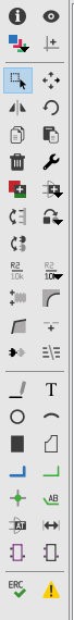
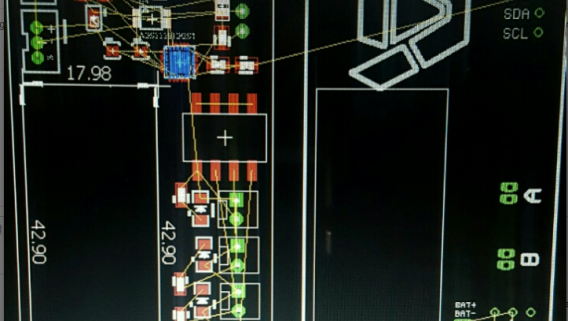
Figure 1: Toolbar of the Eagle Schematic
Training 2: Board
The second training was focused on designing the board layout. These are the key points that were went over.
- Layers: Top and bottom
- Routing the layers
- Auto-routing
- Placing the components
- Talk about Female and Male header connections
- Possible restrictions (Size, placements, drill size and trace size)
- DRC command
- Copper pours for GND and PWR
- Effective GND and PWR connection

Figure 2: Toolbar for Eagle Board
Training 3: Practice
This training was focused on applying what was learned. The first practice was done together where a simple low filter schematic was given to design on Eagle.
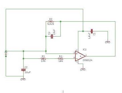
Figure 3: Low Pass Filter Schematic using Operational Amplifier
After the first practice, the second assignments were given as homework. The second assignment given was to design an I/O expander circuit.
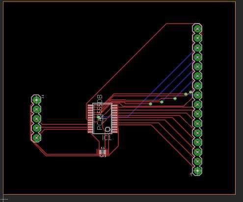
Figure 4: Board Design of I/O Expander HW assignment
Training 4: Quiz
For the last part of the application, I assigned two quizzes. Each quiz was 40 minutes long and were given a simple circuit to design on the schematic and board. There were certain restrictions such as the mil size, the placement of the connectors, the size of the board, and the components’ packages. The grading criteria is the following:
- Did you follow the schematic?
- Did you follow the instructions? (such as package size)
- Is the position of the connectors appropriate?
- The overall quality
- Did you route everything?
- Did you ground the board or did you add the copper pours?
- Did you make it compact as possible? (Within the given size)
The first quiz was an IR sensor and the second is the boost converter. The schematics are shown below
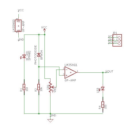
Figure 5: Quiz 1, IR sensor
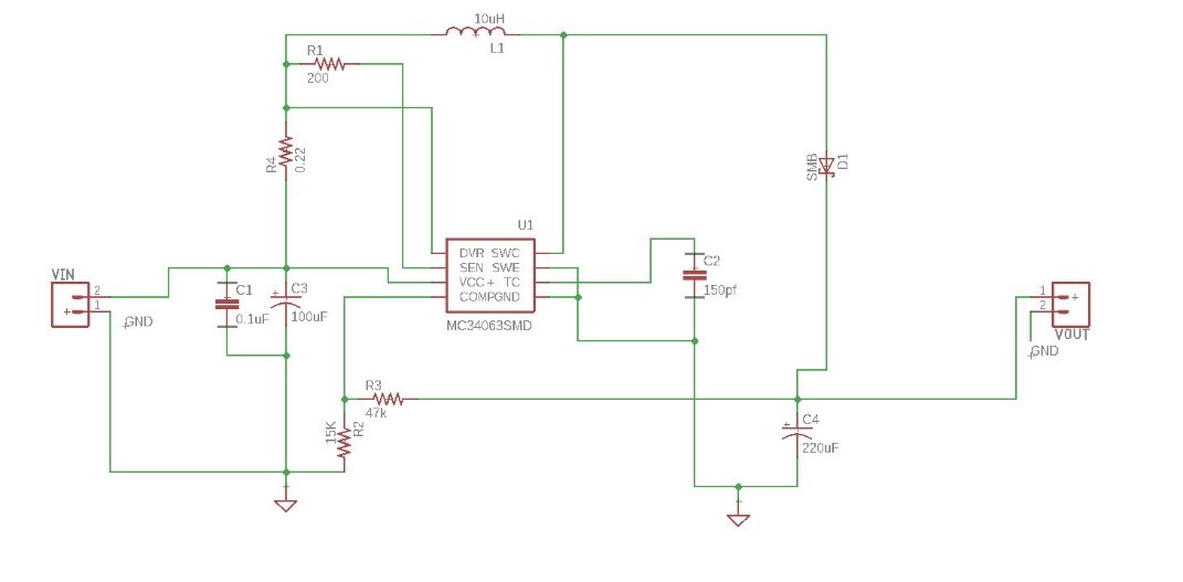
Figure 6: Quiz 2, Boost Converter
References
Spring 2018: Project Power Budget Template
By: Raymundo Lopez-Santiago (Mission, System, and Test)
Verified by: Eduardo De La Cruz (Project Manager and Manufacturing Engineer)
Approved by: Miguel Garcia (Quality Assurance)
Introduction
This blog post covers the 3DoT project power budget. With the design of the version 6.43a of the 3DoT board, the existing power template from last semester needed to be updated. A major change from the last revision to this version is the parameters of the buck/boost converter. The previous revision had the output of the converter at 5V. This current revision has the converter output 3.3V to be used for peripherals needed for each robot project. This revision utilizes the same TPS61200 converter. The battery that will be used is the RCR123A 650mAh, 3.6V Li-Po. The project power budget template version 6.xx has been updated with the help of Professor Hill and Ryan Nguyen.
Project Power Budget (Updated 04/17/18)
Components of the 3DoT can be found in the schematic for the version 6.43a of the 3DoT board. For the schematic, click the following link: 3DoT v 6.43a Schematic.
This version updates the categories defined in the previous version. These categories include the LDO at 3.3V and output from the battery. The LDO incorporates the internal circuitry of the 3DoT board, sensor shield, and header shield. Output from the battery at the rated 3.6V can be used for motors/servos.
The complete power budget spreadsheet can be seen by clicking the following link: 3DoT Project Power Budget Template.
The user can input valued for peripherals used in the correct section. Any sensors should be added to the sensor shield or header section. Motors should be added in the Vout section. See Fig. 2 for clarification. Values inserted for current draw should ones from measurement but values from datasheets will be a good start.
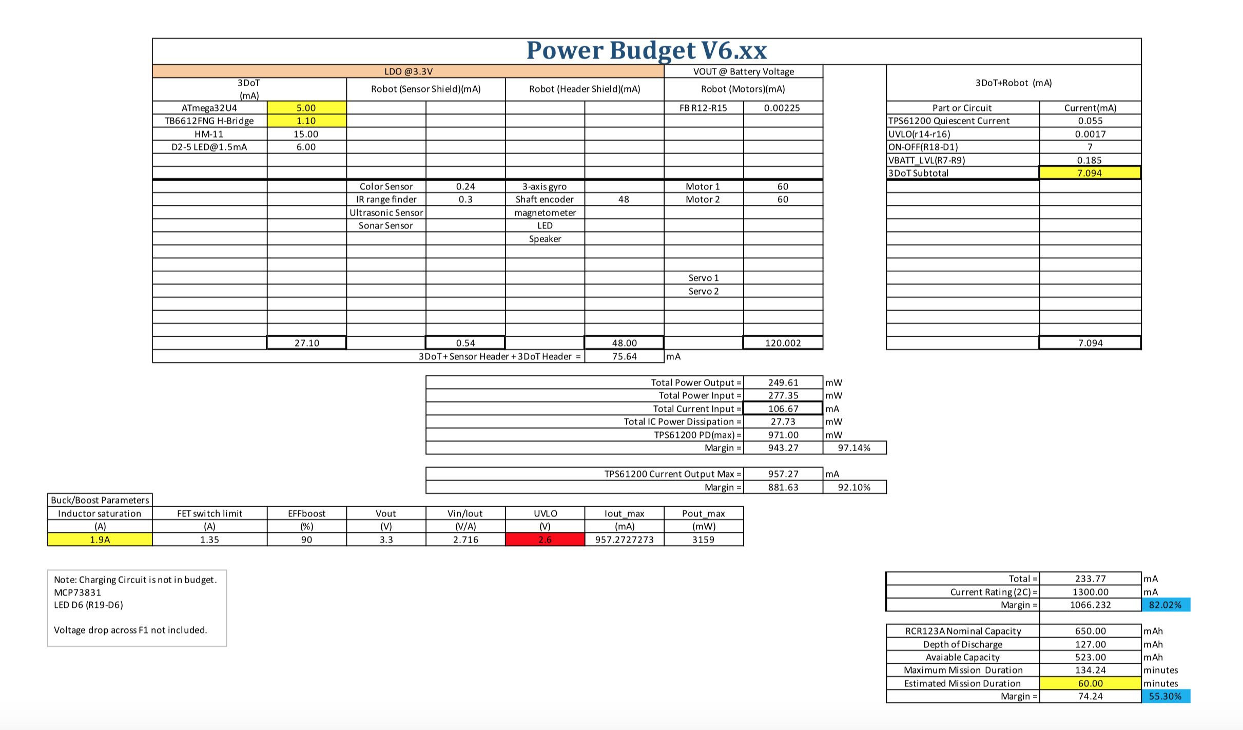 Fig. 1: Spring 2018 3DoT Project Power Budget
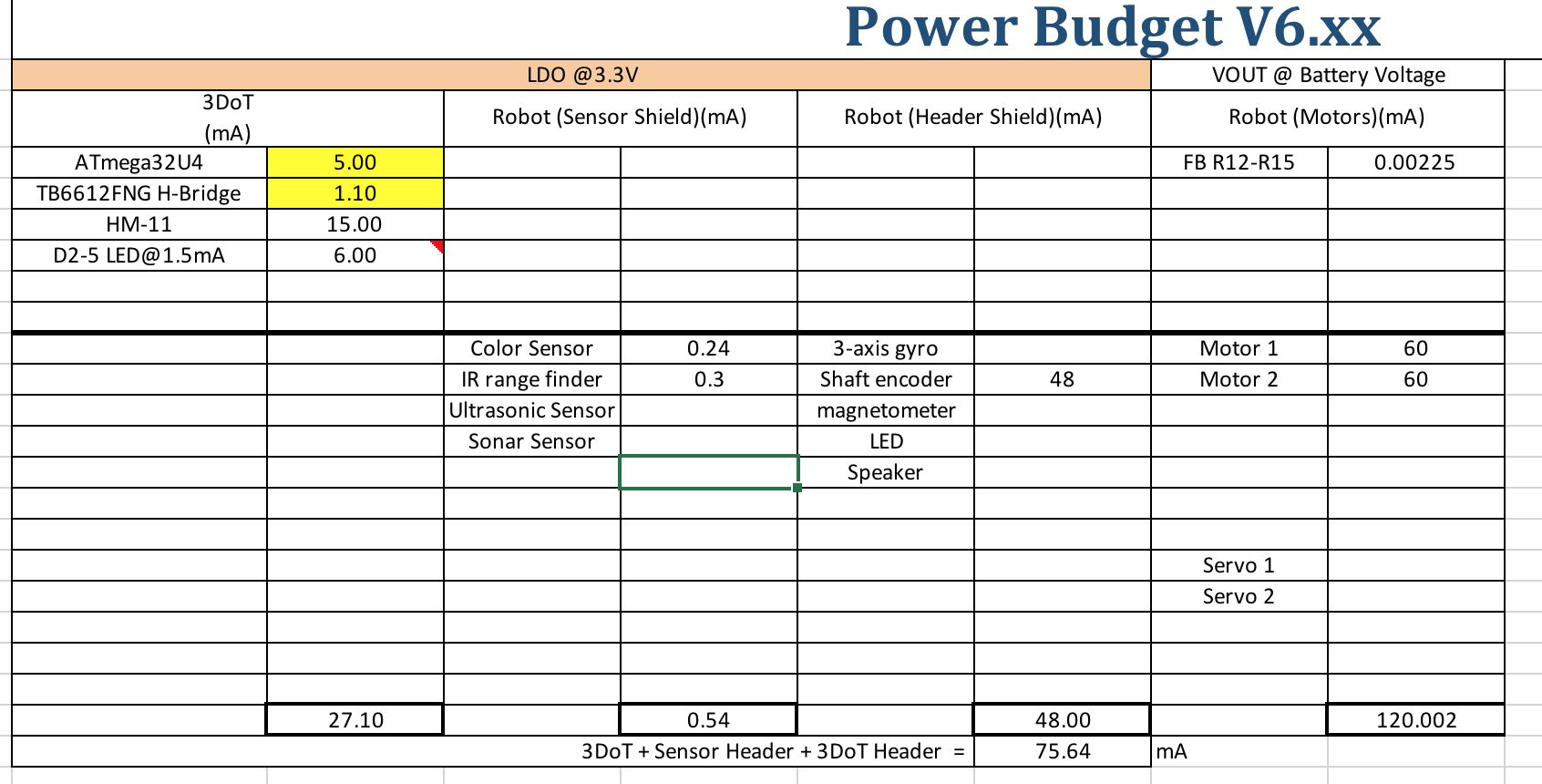
Fig. 2: LDO @3.3V and Vout @ Battery voltage section
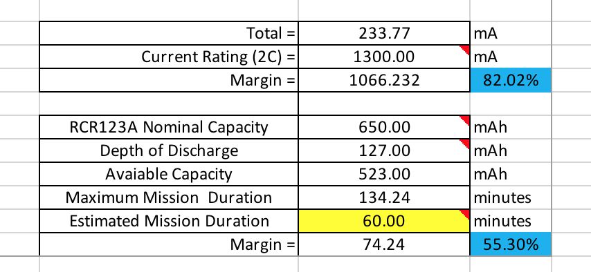 Fig. 3: Calculations for current draw and mission duration
Conclusion
The objective of this power template is to allow each project team to record all peripherals used in their project and their current draws. This template helps identify all current draws so the robot can operate efficiently without exceeding the battery values. Once all the values are inputted for each respective peripheral device used, calculations are automatically updated. The calculations are displayed towards the bottom of the document, see Fig. 3. All the information calculated includes total current draw and the maximum mission duration which is defined differently for each project.
References
- https://docs.google.com/spreadsheets/d/17oXC8C9Apr0KN9fGo3VRT38ZHFaBRNQnUWpWSYL1bdw/edit#gid=205608523
- http://www.ti.com/lit/ds/symlink/tps61200.pdf
- http://ww1.microchip.com/downloads/en/DeviceDoc/Atmel-7766-8-bit-AVR-ATmega16U4-32U4_Datasheet.pdf
- https://drive.google.com/file/d/18xenQLRR–v6t-eWHHrI-9tyA8uVhRLa/view
- https://www.arxterra.com/news-and-eventsmembers3dot-robots3dot-goliath/

3Dot Advanced Lab
In the “Blink” example the frequency at which the LED blinked was controlled by the calls to the delay function. In this lab a potentiometer is used to increase and decrease the duty cycle of an external LED. Concepts introduced in this lab include wiring an external circuit to the 3DoT I2C connector, plus Arduino […]