How to Make a Shield in Eagle CAD
Table of Contents
Introduction
So you want to design a shield for your 3DoT board. First, which shield do you want to design? The 3DoT boards includes both a top “3DoT Shield” and front facing “Sensor Shield.” The 3DoT Shield is typically used to add functionality to the board; for example an accelerometer, gyro, Inertial Measurement Unit (IMU), compass, boost converter, or current monitor etc.. The sensor shield is typically used to add a downward facing sensor; for example an IR sensor, RGB color sensor, or CCD camera. This post shows you How to Design the 3DoT Shield.
The 3DoT Shield plugs into a 16 pin header and typically communicates with the Micro-controller Unit (MCU) via a serial communication protocol. The shield supports I2C, USART, and SPI serial interfaces.
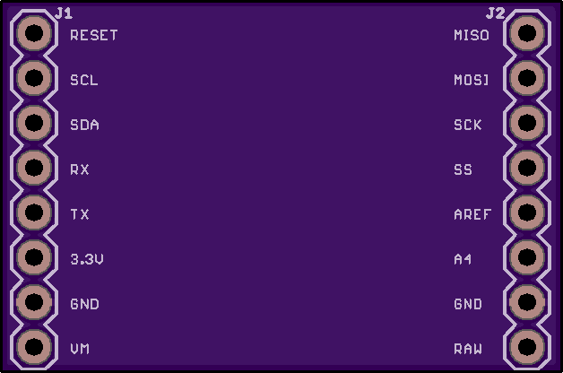
Figure 1: 3DoT Shield
In most cases the pins may also be used to implement a simple digital interface. It also can output a PWM (AnalogWrite) waveform or read an analog input (AnalogRead).
| Pin | Serial Pin | Digital Pin Name | Note |
|---|---|---|---|
| 2 | SCL | D3 | PWM Output |
| 3 | SDA | D2 | |
| 4 | RX | D0 | |
| 5 | TX | D1 | |
| 16 | MISO | D14 | |
| 15 | MOSI | D16 | |
| 14 | SCK | D15 | |
| 13 | SS | D17 | RXLED |
| 11 | A4 | A4 | May be used as digital pin |
In the following tutorial, I will show you how to design and layout a basic 3DoT Boost Shield by starting from an existing open source design.
Setup
This tutorial assumes you have a basic working knowledge of Eagle CAD. If you are new to Eagle CAD you may want to start by reading the blog posts on the Getting Started/Electronics and Control Resources page in the “PCB Design” Section. Before you begin, make sure your computer is configured with the latest software.
- Download and install Eagle CAD
- Download and place in Eagle CAD dru folder OshPark Design Rules
![]()
3DoT Boost Shield Tutorial
So what functionality do you want to add to your robot? To travel in a straight line or turn you may want to add a gyro, compass, and/or rotary (also known as a shaft) encoders. To run 5 or 6 volt motors or servos consider adding a boost converter. If you do add a boost converter, you will want to make sure you do not exceed the 1.3 A capability of the CR123A Li-Ion battery by including a current sensor. Technical Note: The current limit of the 3DoT Power Management IC (PMIC) chip is set to 1.0 A.
In many instances, you can download Eagle CAD layouts and simply adjust the form factor and pin assignments to make your 3DoT shield. Eagle CAD designs are provided by the Arduino Community, Digi-Key Designer, and SparkFun.
For my tutorial, I am going to make a 5v boost converter based on the SparkFun LiPo Charger/Booster – 5V/1A.
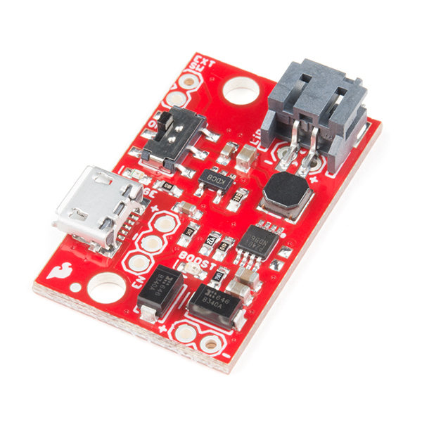
Figure 2: SparkFun LiPo Charger/Booster
So lets begin.
Step 1 – Download: Download the Eagle Files found here. Make a copy of the folder and rename the board (.brd), and schematic (.sch) files and the folder 3DoTBoost5V1A_v1. As you work on your design remember to save often.
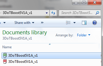
Figure 3: Name Folder and Files
Step 2 – Replace the Frame: Open your soon to be new 3DoT shield in Eagle CAD. Delete the SparkFun Frame and replace it with the FRAME-A4L device found in the SparkFun-Aesthetic Library. Follow these instructions to set the CNAME, DESIGNER, and CREVISION values in the title block:
- Right click the origin of the title FRAME (Small red cross seen near the bottom-left of Figure 4) and select Attributes from the pop-up menu.
- Click the New button.
- Enter the name you want to change, in the example “CREVISION”
- Enter the value you want displayed, in the example “1.0”
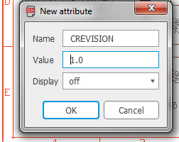
Figure 4: Update Title Block
Step 3 – Simplify the Schematic: The 3DoT board includes a Li-Ion Battery charger so we can delete the top half LiPo Charger Booster of the schematic leaving the Switching Regulator Circuit. We are going to be switching from the SparkFun breakout board connectors to our 3DoT headers so you can delete Jumpers J5, and J6.
Step 4 – Simplify the Board Layout: Now lets cleanup the original Sparkfun Charger/Booster layout shown in Figure r5 by removing artwork, vias, and traces that are now longer applicable.
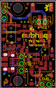
Figure 5: SparkFun Charger/Booster
- Show Layers 21 tPlace and 22 bPlace ONLY (verify layers 39 tKeepout and 40 bKeepout are Hidden). Block select everything and delete. Don’t worry, artwork that is associated with components will not be deleted. Show the layers you just hid. The board should now look like Figure 6 “Boost Only.”
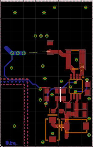
Figure 6: Boost Only
- Rename v10 on bottom layer v1.0.
- Remove unused “shield” polygon.
- Restore Top and Bottom GND polygons to rectangles with dimensions equivalent to the board.
- Remove ground traces and vias that are outside the boost circuit. If they are not already visible show layers 23 tOrigins and 24 bOrigins.
- Block select Boost Circuit and move closer to the left of the board.
Your board should now look similar to Figure 7.
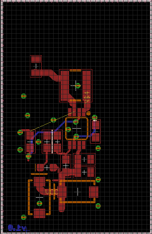
Figure 7: Cleaned-up Board
Congratulations, your design is now ready to be configured as a 3DoT Shield.
Step 5 – Add 3DoT Shield:
The 3DoT Shield with dimensional information is shown in Figure 7. Follow these instructions, to place your boost circuit on the 3DoT Shield. Don’t panic if the circuit does not fit inside the 3DoT shield. We will be working on this problem after we wire up the connectors.
- Redefine your boost shield’s border plus top and bottom ground planes as defined in Figure 7.
- From the SparkFun-Connectors-8pin library add two (2) CONN_08>CONN_08″ devices. They should automatically be labeled J1 and J2.
- Place J1 (left) and J2 (right) in the orientation and location defined in Figure 8.
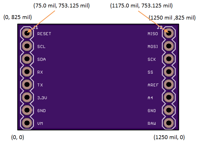
Figure 8: 3DoT Shield with Dimensional Information
Step 6 – Wire Boost Circuit to 3DoT Shield Connectors: Open the schematic window. For our boost circuit we only need to wire the input J2 pin 8 RAW and output J1 pin 10 VM to our circuit. RAW is wired to our battery through a Power Management IC (PMIC) chip. The PMIC in turn is enabled by the switch on the 3DoT board. The VM pin is wired to the motor driver and servo power connectors.
- Add and Name traces VM, RAW, and two GND pins on J1 and J2 as shown in Figure 8 (bottom right). The attractive label symbols are enabled by checking the xref box in the symbols property window. Notice that relative to the J1 and J2 connectors, the input (RAW) is on the right and the output (VM) on the left.
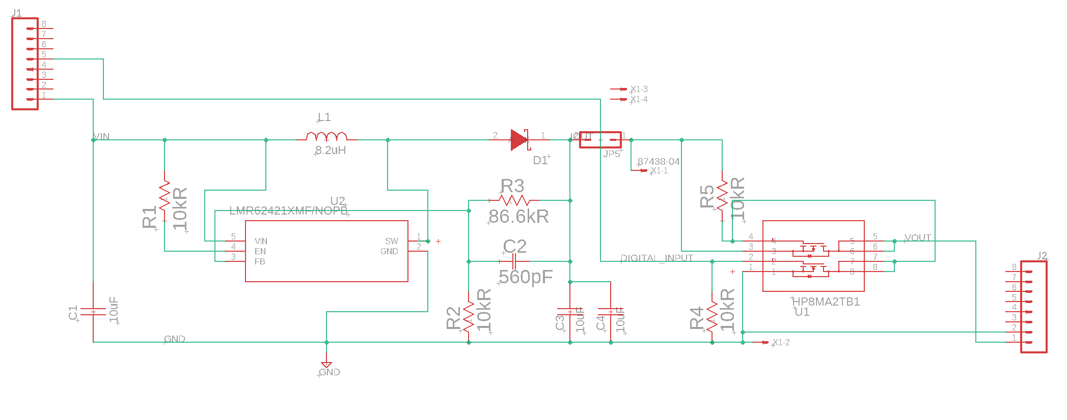
- Returning to the boost schematic. Rename VBATT -> RAW and VCC -> VM. Add labels and clean-up the design. Notice that relative to the circuit, the input (RAW) is now on the left and the output (VM) is now on the right. My final circuit is shown in Figure 9.
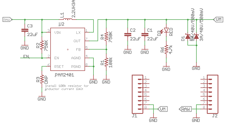
Figure 9: 3DoT Boost Shield Schematic
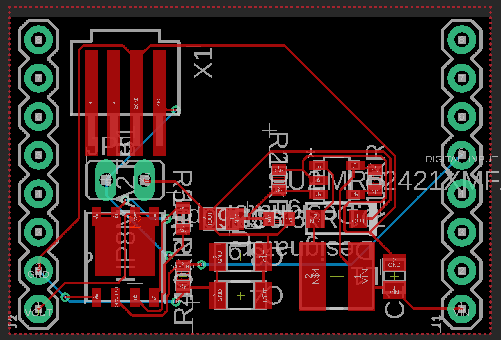
Step 7 – Complete the Board Layout: Switch to the board view window.
- You should now see the layout of the boost circuit connected to the J1 and J2 connectors by air wires (layer 19 Unrouted). With a little tilt of your head you hopefully can see that with a simple rotation to the right (clockwise) the circuit will line up quite nicely with connectors.
- Run 32 mil traces for VM and RAW. Because I am never happy with good enough, I used polygon fills for the VM and RAW traces. Do not forget to name the polygon. For my design I needed to also change the rank of the polygon fills to 1, and the top plane to 2.
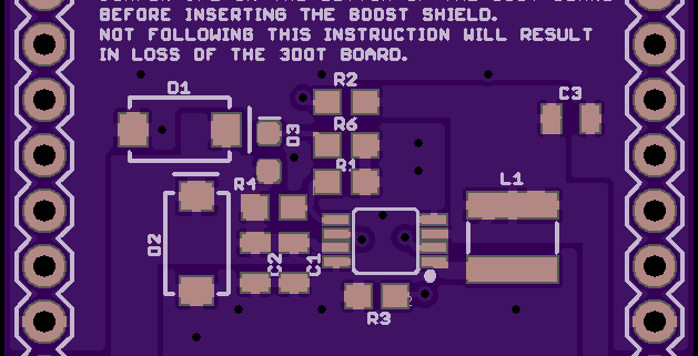
- Although the 3DoT Board is designed to support a Boost Shield, unless the solder bridge across Jumper 1 is removed, a short will occur when the boost shield is plugged in destroying the 3DoT board! To make sure the user is aware of this potential danger to the board, add a note on Layer 21 tPlace with the following text “IMPORTANT: REMOVE SOLDER BRIDGE ACROSS JUMPER J1 ON THE BOTTOM OF THE 3DOT BOARD BEFORE INSERTING THE BOOST SHIELD. NOT FOLLOWING THIS INSTRUCTION WILL RESULT IN LOSS OF THE 3DOT BOARD.“
- Congratulations you have just made your first 3DoT shield!
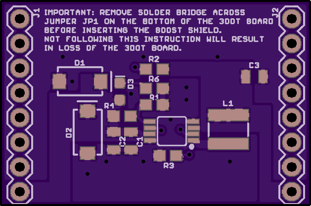
Figure 10: 3DoT Boost Shield PCB
On your Own
While my design is good it could be better. Here are two modifications you can make to improve your boost shield.
- Assign one of the unused serial interface pins as a digital pin and wire to the EN trace. Now you can turn the boost circuit on and off through software. This is especially important if you want to avoid a large an inrush of current when the 3DoT board is initially turned on and to save power when the motors are off.
- Add a current sensing circuit to your shield. Whenever you run motors and servos, especially with a boost circuit, it is important to manage the amount of current drawn by the robot. For example, to turn off the motors if one of them stalls resulting in excessive current being drawn which will result in the loss of the motor and potentially the 3DoT board as well.