Card Reader PCB Shield Design – Spring 2021
Author/s: Reza Tajik
Table of Contents
Choosing Sensor
According to my research as a card reader in the Maze project, I came up with three different camera sensors (Pixy2, Husky Lense Gravity & Jevois A33), but none of them were completely hardware and software open-source then I found “ESP32 with Camera Module OV2640” which was an open-source camera (hardware& software). In fact, the main reasons to come up with camera sensor is that I found it more accurate to identify the images (image recognition) by processing the image. Besides, scanning the QR code and color detecting were other reasons that could be done by camera. Since I should have designed my PCB in this course, I watched different breakout board design videos in YouTube channel, to get more ideas for my PCB design which was helpful.
OV2640 Camera
The camera module that I considered using is OV2640 which easily can be connected to the chosen shield (ESP32). In fact, this camera has the following feature that is good enough to use for identifying objects. It is a 2 Megapixel camera, exceedingly small, different output formats, image transfer rate(60ps).
You can find more details at the following link:
ESP32-CAM Video Streaming Web Server (works with Home Assistant) | Random Nerd Tutorials
https://dronebotworkshop.com/esp32-cam-intro
Schematic Design
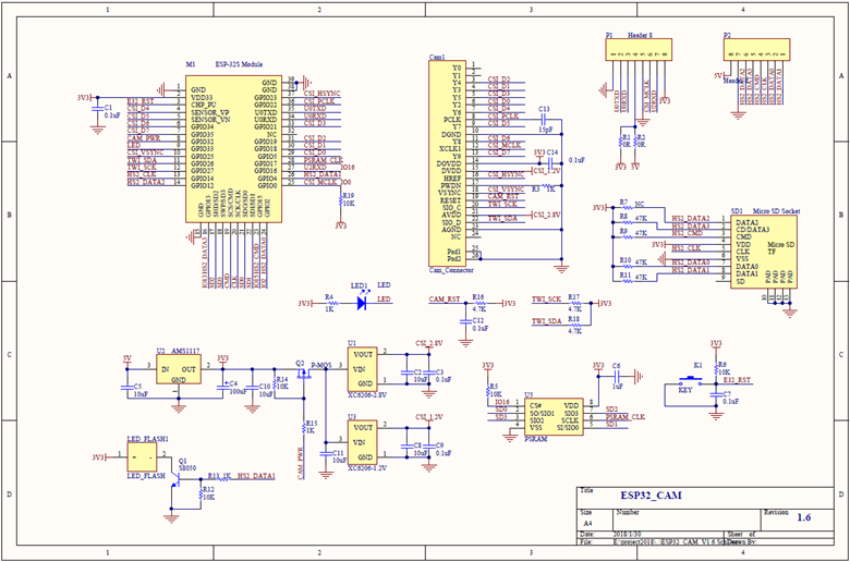
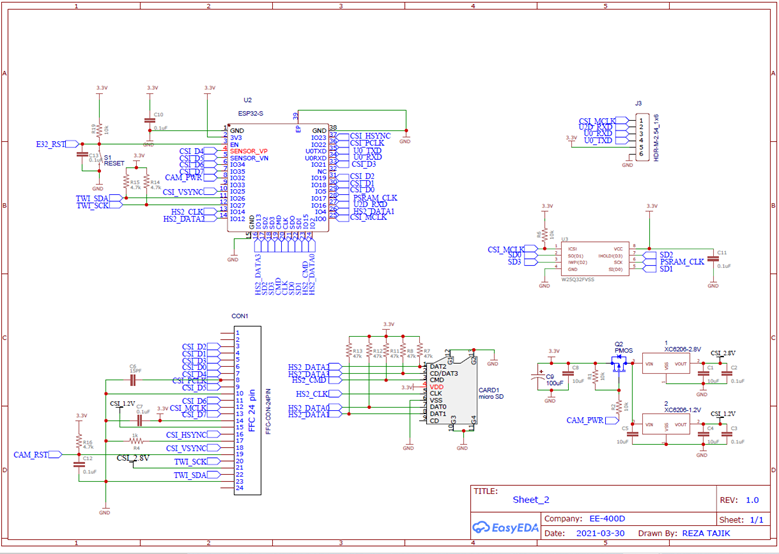
I selected the ESP32 board not only because of the following information: small in size, computing speed, 520KB SRAM, external 4MPSRAM, Supports UART/SPI/I2C/PWM/ADC/DAC, Support OV2640 and OV7670 cameras, built-in flash lamp, Support for serial port local but also easy to program with Arduino IDE and has an open-source board that gives me the ability to use the existing schematic to get the idea for my design. In fact, I tried to simplify the schematic by removing some parts such as the 5V regulator (since 3DOT support 5V and 3.3 V), Flash LED, and extra pins which were not necessary for my shield. Indeed, I designed my PCB in EagleCAD software. Finally, after getting design approval, I ordered my PCB through some companies such as JLCPCB, OSH Park, etc.
PCB Design
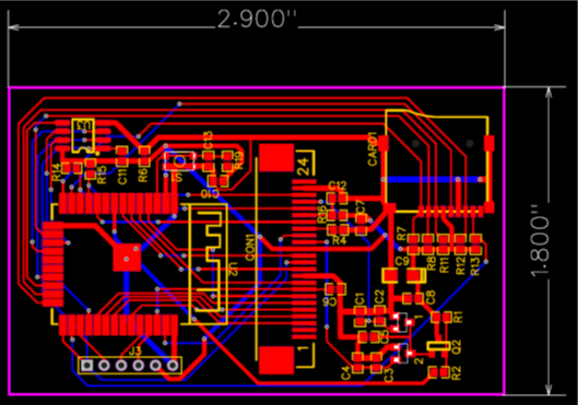
The following figure is the final PCB design that took me about 14 days to be done completely. It was a challenge for me to reach this point. PCB_PCB_Reza-Tajik_2021-04-02 (2)
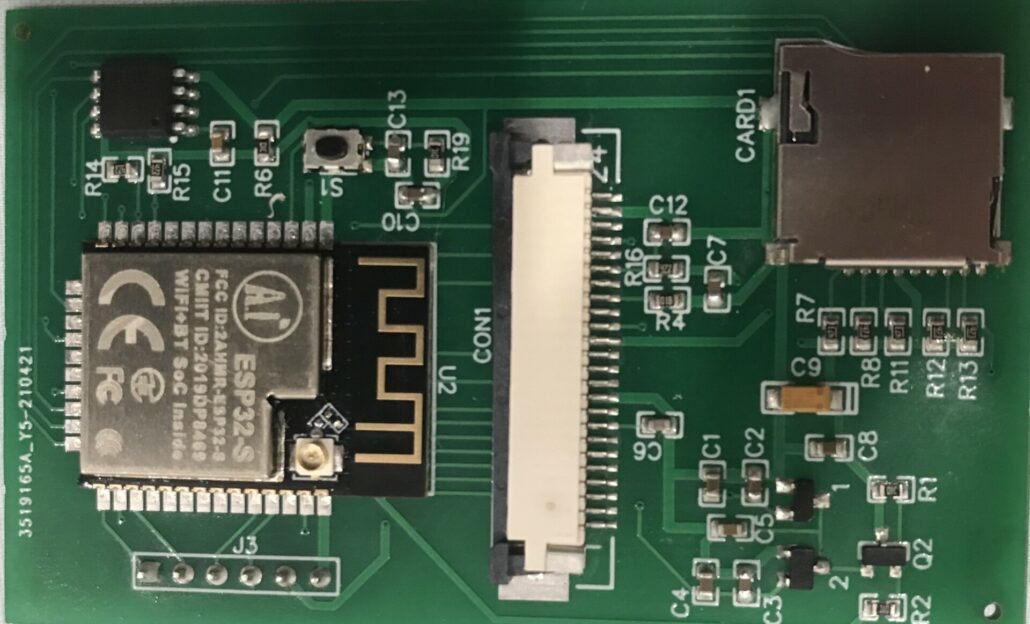
The camera shield PCB has shown in the following figure.
Conclusion
To conclude, I would like to say that all these steps from the beginning to the end, taught me how the design process works and show me a new face of electronics and robotic as well as a perspective for future design.
References/Resources
- ESP32-CAM Video Streaming Web Server (works with Home Assistant) | Random Nerd Tutorials
- https://dronebotworkshop.com/esp32-cam-intro
