UFO PCB Layout Spring 2016
Posted by: Luis Valdivia (Project Manager)
Written by: Juan Mendez (Manufacturing Engineer)
Table of contents
Introduction
Wire Traces
Building the PCB
Introduction
Our PCB was laid out after the schematic that was provided by our electronics and control engineer. The size of the board was set to roughly 2.5 by 2.5 inches so it can fit on the UFO frame. The screw holes were spaced out roughly 1.8 inches apart from each other. The reason this was done was to have the ability to put the multiwii on top of the pcb or vice versa. Each component was organized based on the size of the component and following recommendations from the spec sheets. Components such as the battery alarm pin headers were spaced out because alarm was approximately 3 mm thick.I isolated it from everything else so spacing would not be an issue. The servo pin headers were spaced out evenly at roughly 2 mm apart so spacing would not be an issue when being connected to the servos. The buck converter was placed close to the input voltage pads. I placed ground vias on the thermal pad of the buck converter since it was recommended by the spec sheet. Components such as the capacitors and diodes were placed next to switching output pins in order to reduce magnetic noise. The output capacitor C3 was placed as close as possible to the inductor and diode to reduce noise and to increase efficiency. Resistors “R2” and “R3” were placed close to the Feedback pin as mentioned in the data sheet. Capacitor “C1” was placed close to the enable pin and to ground as recommended on the data sheet. The pin headers for the bluetooth connections were put in the bottom so they would not get in the way of anything else similarly to the battery alarm. Lastly the Servo driver was placed close to the servo pin headers and the lightshow pin headers were added on the top left corner of the board.
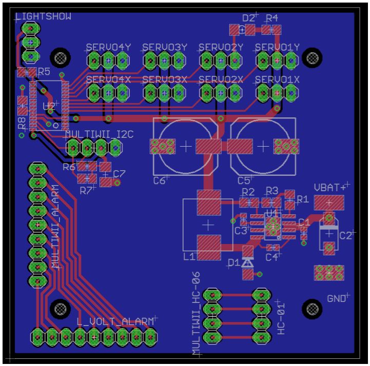
Figure 1.1 .BRD layout of PCB on Cadsoft Eagle
Wire Traces
In order to make sure that mistakes were not repeated from previous semesters, we used a trace width calculator from 4PCB to calculate how thick the traces had to be. Each servo was going to be drawing a max of two amps. The board thickness was roughly 1 ounce. According to the trace calculator, the traces had to be roughly 2.03 mm thick in order to draw 2 amps. Other traces were either signal or did not draw enough current and were set to be no more than .5 mm thick.
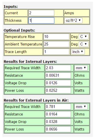
Figure 1.2 Trace width calculator
Building the PCB
After laying out the PCB, we submitted our Layout and schematic to be ordered along with our parts list. With the help of our class president Ryland Watts, we were able to mount on the surface mounting parts using a reflow station in IEEE. We mounted on the small resistors and capacitors first since they could have been done at once with the reflow station that we were using. Since the capacitors were bigger, we had to mount them on one at a time only because if we tried doing them all together, the heat of the reflow station would not reach the pads, therefore not mounting them properly. Once those components were on the PCB, we soldered on the pin headers. One issue we experienced was that the inductor ended up being bigger than we anticipated so the pads on the PCB were too small to mount on the inductor using the reflow station. To fix this, with the help of our electronics and control engineer, we soldered on the inductor and were able to mount on the inductor. Once the PCB was built, it was ready for testing.
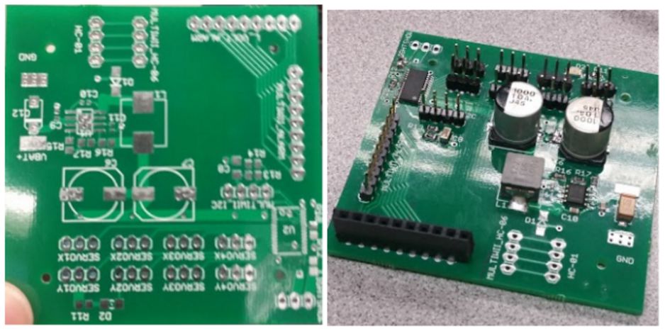
Figure 1.3 PCB before and after all parts have been attached
To view a video of the PCB Buck Converter stepping voltage, Click here
To view a video of the PCB Servo Power Supply, Click here
Reference:
To view the schematic for this PCB check out our blog post: PCB Design: Schematic – Spring 2016


