Midterm II Review Questions
In addition to the following questions, I would recommend reviewing the Midterm 1 Load-Store Worksheet
Warning:
Your one-sided 8 ½ x 11 page of notes may not contain questions and answers or copy-pasted bullet-points. It may only contain technical information relevant to the ATmega processor and other coursework related material. The following questions are provided to help you prepare for the second midterm only.
ATmega328P Timers and Interrupts
1. A computer spends its whole life _________ and _________ instructions.
[expand title=”Answer” tag=”h5″]
Fetch and Execute
[/expand]
2. Where can you find the Interrupt Vector Table (IVT)?
[expand title=”Answer” tag=”h5″]
Flash Program Memory
[/expand]
3. How many words (16-bits) are reserved for each entry in the IVT?
[expand title=”Answer” tag=”h5″]
2
[/expand]
4. While the global interrupt SREG bit I is cleared, both the Timer/Counter 1 Overflow bit is set (IVT Address IVT 0x001A) Timer1 OVF and an external interrupt is received (IVT Address 0x0002) INT0. Assuming the interrupt enable bit for both interrupts is set, what will happen when the global interrupt bit is set (enabled)?
[expand title=”Answer” tag=”h5″]
The External Interrupt Request 0 will be run.
[/expand]
5. In which register can you find the global interrupt enable bit?
[expand title=”Answer” tag=”h5″]
SREG
[/expand]
6. How many bits need to be set for a Timer/Counter 1 Overflow interrupt to be triggered?
[expand title=”Answer” tag=”h5″]
3 (SREG I, TOIE1, TOV1)
[/expand]
7. When an interrupt is triggered, what register is placed on the stack?
[expand title=”Answer” tag=”h5″]
PC
[/expand]
8. Why is this register saved?
[expand title=”Answer” tag=”h5″]
So the currently running process can continue execution when the processor is completes running the ISR.
[/expand]
9. Why is the first instruction executed, at address 0x0000, always a jump?
[expand title=”Answer” tag=”h5″]
So the AVR processor does not accidentally execute an ISR.
[/expand]
10. If the instruction at address 0x0000 is not a jump what ISR will be executed?
[expand title=”Answer” tag=”h5″]
External Interrupt Request 0 INT0 at address 0x0002.
[/expand]
11. What triggers a Timer/Counter 1 Overflow Interrupt?
[expand title=”Answer” tag=”h5″]
Counter goes from 0xFFFF to 0x0000
[/expand]
12. What immediately happens when an interrupt occurs?
[expand title=”Answer” tag=”h5″]
The microcontroller completes the current instruction, stores the address of the next instruction on the stack, and clears the SREG I-bit.
[/expand]
13. Just before a Timer/Counter Overflow Interrupt is run, what IVT address needs to be placed in the program counter (PC)?
[expand title=”Answer” tag=”h5″]
0x001A
[/expand]
14. What is instruction is required to return from an Interrupt?
[expand title=”Answer” tag=”h5″]
reti
[/expand]
15. In what way is a ret instruction different from an reti instruction?
[expand title=”Answer” tag=”h5″]
An reti instruction sets the global interrupt enable flag bit I in SREG.
[/expand]
16. What is one of the last things and ISR does before it returns control to the interrupted program?
[expand title=”Answer” tag=”h5″]
Restores the Program Counter and Enables the global interrupt flag bit I.
[/expand]
17. What is the first and second to last thing your ISR should do?
[expand title=”Answer” tag=”h5″]
Save and restore the SREG register.
[/expand]
18. What is the last thing your ISR should do?
[expand title=”Answer” tag=”h5″]
Execute an reti instruction.
[/expand]
19. What is wrong with this instruction push SREG?
[expand title=”Answer” tag=”h5″]
You can only push a general purpose register onto the stack.
[/expand]
20. Where should your ISR save the SREG register?
[expand title=”Answer” tag=”h5″]
One of the 32 general purpose registers.
[/expand]
21. Where should your ISR save general purpose registers modified by the ISR?
[expand title=”Answer” tag=”h5″]
Registers modified by the ISR should be temporarily placed on the stack.
[/expand]
22. Upon return from an ISR and enabling the global interrupt flag ; the AVR processor finds another interrupt waiting to be executed. What will happen next?
[expand title=”Answer” tag=”h5″]
The main program will execute one more instruction before any pending interrupt is run.
[/expand]
23. How many bits would be required to encode the register direct addressing mode?
[expand title=”Answer” tag=”h5″]
5 because 25 = 32
[/expand]
24. The immediate addressing mode can only access 16 of the 32 general purpose registers. How many bits would be required to encode the register used in this type of instruction?
[expand title=”Answer” tag=”h5″]
4 because 24 = 16
[/expand]
25. The immediate addressing mode encodes the data (operand) with the instruction. How many bits would be required to encode the data?
[expand title=”Answer” tag=”h5″]
8
[/expand]
AVR Addressing Modes including Indirect
1. You can find the operand for the immediate addressing mode in what type of memory?
[expand title=”Answer” tag=”h5″]
Flash Program Memory
[/expand]
2. You can find the operand for the direct addressing mode of an lds and sts instruction in what type of memory?
[expand title=”Answer” tag=”h5″]
SRAM Data Memory
[/expand]
3. You can find the operand for the direct addressing mode of an in and out instruction in which address space(s)?
[expand title=”Answer” tag=”h5″]
SRAM Data Memory and I/O Register Memory
[/expand]
4. The address space of which two addressing modes overlap?
[expand title=”Answer” tag=”h5″]
SRAM Data Direct and I/O Register Memory Direct
[/expand]
5. What addressing mode should you use if you want to look up a pre-defined value in a table (data is known at assembly time)?
[expand title=”Answer” tag=”h5″]
Flash Program Indirect
[/expand]
6. What addressing mode should you use if you want to look up a value in a table (data is known at run time)?
[expand title=”Answer” tag=”h5″]
SRAM Data Indirect
[/expand]
7. What addressing mode is used for the source operand of an lpm instruction?
[expand title=”Answer” tag=”h5″]
Flash Program Indirect
[/expand]
8. What register pair is found in the source operand address field of an lpm instruction?
[expand title=”Answer” tag=”h5″]
Z
[/expand]
9. What register numbers correspond to pre-defined mnemonics ZH:ZL?
[expand title=”Answer” tag=”h5″]
R31:r30
[/expand]
10. What two addressing mode should you use if you want to work with a table of data located in SRAM (data is known at run time)?
[expand title=”Answer” tag=”h5″]
1. SRAM Data Indirect and
2. SRAM Data Indirect with Displacement
[/expand]
11. What addressing mode is used for the source operand of an ld instruction?
[expand title=”Answer” tag=”h5″]
SRAM Data Indirect
[/expand]
12. Which three register pairs may be found in the source operand address field of an ld instruction?
[expand title=”Answer” tag=”h5″]
X, Y, and Z
[/expand]
13. What two 8-bit register mnemonics are used to define the X register pair?
[expand title=”Answer” tag=”h5″]
XH:XL and R27:r26
[/expand]
14. What addressing mode is used for the destination operand address field of the instruction lpm r16, Z?
[expand title=”Answer” tag=”h5″]
The key to this question is in italics “destination.” The destination operand uses the Register Direct addressing mode, the source operand is register indirect.
[/expand]
15. What register is both a source and a destination for the instruction add r16, r17?
[expand title=”Answer” tag=”h5″]
R16
[/expand]
16. Write a code snip-it to load the 3rd byte (index = 2) of data from a table (label = TABLE) located in Flash Program memory. Answer left up to the student.
17. What is wrong with this instruction lds r16, low(Table << 1)? The source operand address field is of the immediate addressing mode type.
[expand title=”Answer” tag=”h5″]
The ldi instruction should have been used in place of the lds instruction.
[/expand]
18. I want to load the number 3316 into register 16. Why can I not use the instruction lds r16, 0x33 to do this?
[expand title=”Answer” tag=”h5″]
The source operand address field should be immediate , not SRAM Data direct. The lds instruction would load r16 with the contents of SRAM memory at location 0x33. The ldi instruction should have been used in place of the lds instruction.
[/expand]
19. What addressing mode is used for the destination operand address field of the instruction lds r16, 0x33?
[expand title=”Answer” tag=”h5″]
Register Direct
[/expand]
20. The AVR processor saves bytes of data in Flash Program Memory using what memory byte ordering?
[expand title=”Answer” tag=”h5″]
Little Endian
[/expand]
21. Big Endian saves what half of a 2 byte (16-bit) word in the first byte (lowest address)?
[expand title=”Answer” tag=”h5″]
The most significant (Big) byte.
[/expand]
22. What addressing mode is great for implementing look-up tables in Flash Program Memory?
[expand title=”Answer” tag=”h5″]
Program Memory Indirect
[/expand]
23. Build a program to convert a 4-bit gray-code number into binary. Solution left to the student
24. What instruction is used to divide a register by two?
[expand title=”Answer” tag=”h5″]
lsr
[/expand]
25. Write a program to set a 32 byte buffer located in SRAM to the blank ‘’ ASCII character. Solution left to the student.
26. To modify the seven segment display on the proto-shield you must write to register 8 and do what?
[expand title=”Answer” tag=”h5″]
call spiTx
[/expand]
AVR Branching and Looping
1. ISA is an abbreviation for what?
[expand title=”Answer” tag=”h5″]
Instruction Set Architecture
[/expand]
2. How many general purpose registers does the AVR processor have?
[expand title=”Answer” tag=”h5″]
32
[/expand]
3. What is the mnemonic for the last AVR general purpose register?
[expand title=”Answer” tag=”h5″]
r31
[/expand]
4. All unconditional jump instructions using the relative addressing mode, utilize 12 bits to encode the distance the program is to jump relative to the program counter (PC). Given that this 12 bit number is saved using 2’s complement notation, what is the range in words (16-bits) that the AVR processor can jump for this type of instruction?
[expand title=”Answer” tag=”h5″]
Branch relative to PC + (– 2k-1 a 2k-1– 1, where k = 12) + 1 aPC-2048 to PC+2047, within 16 K word address space of ATmega328P
[/expand]
5. All conditional branch instructions using the relative addressing mode, utilize 7 bits to encode the distance the program is to branch relative to the program counter (PC). Given that this 7 bit number is saved using 2’s complement notation, what is the range in words (16-bits) that the AVR processor can branch for this type of instruction?
[expand title=”Answer” tag=”h5″]
All branch relative to PC + (– 2k-1 a 2k-1– 1, where k = 7) + 1 aPC-64 to PC+63, within 16 K word address space of ATmega328P
[/expand]
6. Which instructions do you typically find before a relative branch instruction? Compare and test instructions?
[expand title=”Answer” tag=”h5″]
cp, cpc, cpi, tst, bst
[/expand]
7. Compare and test instructions like cp, cpc, cpi, tst, bst do not modify any of the 32 general purpose registers. What register(s) do they modify?
[expand title=”Answer” tag=”h5″]
SREG
[/expand]
8. What type of instruction typically follows a compare and test instruction, like cp, cpc, cpi, tst, bst?
[expand title=”Answer” tag=”h5″]
A conditional control transfer instruction.
[/expand]
9. Why does a compare or test instruction, typically precede a conditional branch instruction?
[expand title=”Answer” tag=”h5″]
The compare or test instruction sets or clears flag bits within the status register (SREG) used by the conditional branch instruction to make a decision.
[/expand]
10. What is wrong with the following two sequential instructions? cpi r16, 0x33,followed by rjmp there
[expand title=”Answer” tag=”h5″]
The first instruction is setting and clearing SREG bits to be used by a conditional branch instruction. The second instruction is an unconditional jump instruction which doesn’t need to make any decision (i.e., it is always going to jump).
[/expand]
11. Why is the following two sequential instructions silly?
[expand title=”Answer” tag=”h5″]
clr r16,followed by ldi r16, 0x33 The second instruction will write 3316 to r16, so there is no reason to clear it.
[/expand]
12. What bit(s) within SREG are never modified by a compare or test instruction?
[expand title=”Answer” tag=”h5″]
I (global interrupt enable), T (bit copy storage).
[/expand]
13. What is wrong with the following two sequential instructions? cpi r16, 0x33,followed by brts there
[expand title=”Answer” tag=”h5″]
The first instruction is setting and clearing SREG bits associated with an ALU instruction. The second instruction is a conditional branch instruction which tests to see if the T-bit is set. The T-bit is not modified by a compare instruction.
[/expand]
14. Assuming that r16 contains the value 0x33. What value would be in r16 after the instruction cpi r16, 0x33 is executed?
[expand title=”Answer” tag=”h5″]
R16 = 0x33
[/expand]
15. Assuming that r16 contains the value 0x33. What value would be in r16 after the instruction subi r16, 0x33 is executed?
[expand title=”Answer” tag=”h5″]
R16 = 0x00
[/expand]
16. Assuming that r16 contains the value 0x33. What 1-bit value would be contained in the Z-bit in SREG after the instruction cpi r16, 0x33 is executed?
[expand title=”Answer” tag=”h5″]
Z = 1
[/expand]
17. What type of instruction never modify bits within the SREG register?
[expand title=”Answer” tag=”h5″]
Data Transfer
[/expand]
18. Write the code to implement the following flow-chart
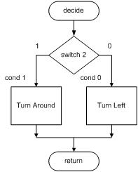
Solution left to the student
19. Write the code to implement the following flow-chart
Solution left to the student
AVR Bits and Bytes
1. What instruction(s) could you use to clear the carry bit?
[expand title=”Answer” tag=”h5″]
clc, bclr
SREG_C, bclr 0
[/expand]
2. What instruction would you use to clear PORT D bit 3?
[expand title=”Answer” tag=”h5″]
cbi
PORTD,3 or cbi 0x0B,3
[/expand]
3. What is wrong with this the instruction cbi TIMSK1, 0?
[expand title=”Answer” tag=”h5″]
TIMSKI is located in the extended I/O address space of the ATmega328P microcontroller and is therefore not accessible.
[/expand]
4. Write
an instruction to clear bit 4, 2, and 0 in register 16.
[expand title=”Answer” tag=”h5″]
cbr r16,
0b0001 0101
[/expand]
5. Write an instruction to clear bit 4, 2, and 0 in register 16 without using the cbr instruction.
[expand title=”Answer” tag=”h5″]
andi r16, 0b1110 1010 or and r16, 0xEA
[/expand]
6. Write an instruction to set bit 4, 2, and 0 in register 16.
[expand title=”Answer” tag=”h5″]
sbr r16, 0b0001 0101
[/expand]
7. Write an instruction to set bit 4, 2, and 0 in register 16 without using the sbr instruction.
[expand title=”Answer” tag=”h5″]
ori r16, 0b0001 0101 or and r16, 0x15
[/expand]
8. What is wrong with this instruction to toggle bit 4, 2, and 0 in register 16?
[expand title=”Answer” tag=”h5″]
eor r16, 0b0001 0101
The eor instruction works with two registers.
[/expand]
9. Write an instruction sequence to toggle bit 4, 2, and 0 in register 16.
[expand title=”Answer” tag=”h5″]
ldi r17, 0b0001 0101
eor r16, r17
[/expand]
10. Write an instruction sequence to set bits 4, 2, and 0 to 1012 in register 16, without modifying any other bits.
[expand title=”Answer” tag=”h5″]
cbr r16, 0b0000 0100
sbr r16, 0b0001 0001
[/expand]
11. Write an instruction to set bits 7, 6, 5, 4, 3, 2, 1, 0 in register 16, without using the sbr or or instruction.
[expand title=”Answer” tag=”h5″]
ser r16
[/expand]
12. Write a program to wire switch 0 to the decimal point of the 7-segment display on the proto-shield.
Solution left to the student
13. Pulse Clock input of Proto-Shield Debounce D Flip-flop (PORTD bit 5). Assume currently at logic 0.
[expand title=”Answer” tag=”h5″]
sbi PORTD, 5
cbi PORTD, 5
[/expand]
14. What logical instruction is implemented by the tst instruction?
[expand title=”Answer” tag=”h5″]
and
[/expand]
15. What is the difference between the and and the tst instruction?
[expand title=”Answer” tag=”h5″]
The tst instruction performs the and operation without modifying the destination operand.
[/expand]
16. What does the cp instruction have in common with the tst instruction?
[expand title=”Answer” tag=”h5″]
Both do not modify the register(s) in the operand field. Both are used to set flag bits in SREG.
[/expand]
17. Assuming register 16 contains 0x00. What would the Z-bit be set/cleared to after executing the instruction tst r16?
[expand title=”Answer” tag=”h5″]
Z = 1
[/expand]
18. What instruction is used to disable all interrupts?
[expand title=”Answer” tag=”h5″]
cli
[/expand]
19. How many operand(s ) does the tst instruction have?
[expand title=”Answer” tag=”h5″]
1
[/expand]
20. Complete the following Boolean expression representing the operation of a the tst r16 instruction.
r16 ___ r16
[expand title=”Answer” tag=”h5″]
r16 ∙r16
[/expand]
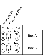
21. What instruction would be used to implement the logic operation represented by the question mark (?) in Figure 1 (Shown below)?
[expand title=”Answer” tag=”h5″]
eor
[/expand]
22. What phrase best describes the operation shown in Figure 1 box A?
[expand title=”Answer” tag=”h5″]
Don’t Change
[/expand]
23. What word best
describes the operation shown in Figure 1 box B?
Figure 1
[expand title=”Answer” tag=”h5″]
Toggle
[/expand]
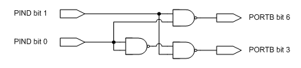
24.
Write the code needed to implement the following circuit.