Spring 2018 AT-ST Walk Code

By: Samuel K Yoo (Electronic & Control – Software)

Verified By: Intiser Kabir (Project Manager)

Approved By: Miguel Garcia (Quality Assurance)

Table of Contents

Introduction

During the creation of AT-ST, this is a program that allows AT-ST to walk. Note that this program is used for the current model and might need to be updated later on. The code is very straightforward as it only uses the motor and controls the speed. There are commented code for the servo to make it shift the weight of the bot.

Code

Figure 1: screenshot of code pt 1

Figure 2: Walk Code pt 2

Explanation

This code should not be used in the future irritations of the AT-ST. The major explanation of why it should not be used it because of the code being adjusted with some physical deformities with the leg. If the future irritations are going toused this AT-ST, then the code should be used to make the robot walk. However, a more appropriate approach to creating a walking motion code is setting the AIN pins and BIN pins to clockwise and counterclockwise. Keep in mind if the robot is facing you, the left motor must spin counterclockwise and the right motor must spin clockwise. The AIN pins should be programmed to the right motor and BIN pins should be the same with the left motor. To program the motor for a motor driver this table should be used

Figure 3: Table for motor control

The PWM should also be tested on each motor to determine what speed the motors are truely rotating at. This can be done with the shaft encoder, which I have not programmed with. There will be a link in the References for those who would want to learn how to program it.

References

  1. https://roboticbasicsblog.wordpress.com/tag/rotate/
  2. https://playground.arduino.cc/Main/RotaryEncoders

Spring 2018 AT-ST Which Way

By: Samuel K Yoo (Electronic & Control – Software)

Verified By: Intiser Kabir (Project Manager)

Approved By: Miguel Garcia (Quality Assurance)

Table of Contents

Introduction

In this code we are creating a which way sub routine. There are two methods of doing this, one being, code one which is the switch case decision. The other method is the index method which saves a huge amount of coding. The method used for the AT-ST is the index method.

Code

Figure 1: Whichway Code Screenshot

Figure 2: Code Screenshot Cont.

Figure 3: Code Continue

Explanation

The maze.h file contains the maze array which should be given in the EE444 lab training, but if not, there would be a link to it in the Reference. The code in the maze.h file also contains the two tables and the structure for the main programs. The enterRoom, turnInMaze, stepInMaze and roomInMaze all use the index. The index moves the values on the table to point at the appropriate row and column for each desired value. This method is really good and saves a lot space as mentioned above.   

References

  1. http://web.csulb.edu/~hill/ee444/Labs/Lab%204%20Arrays/Lab%204%20(C++).pdf
  2. http://web.csulb.edu/~hill/ee444/maze.h

Spring 2018 AT-ST Final Code

By: Samuel K Yoo (Electronics & Control – Software)

Verified By: Intiser Kabir (Project Manager)

Approved By: Miguel Garcia (Quality Assurance)

Introduction

This is the final code for the AT-ST for Spring of 2018. There are many problems with the code, not only with missing sections, but there is also no test for the other values. The robot can walk forward and turn, however, the code to test for the maze has not been done along with missing parts.  

Code

Figure 1: Final Code Screenshot

Figure 2: Continue

Figure 3: Continue

Explanation

This code has a lot of missing code. The biggest code that is missing is from the void loop, which uses the whichway code and the Bluetooth integration. For the future electronic and control engineer of the AT-ST read the 3DoT manual ahead of time. The coding for the bluetooth is extremely difficult. The lab sequence is not that difficult to understand however the bluetooth is. Another advice is to test the robot as quickly as possible to find the errors both in the program and physical movements. The walking program should work immediately, however, a physical error with one of the legs cause a lot of hardships. The code forward only works with the spring 2018 model. The program takes one small step with the messed up leg and four to five steps with the good leg. This will cause it to steer toward a direction, however, it still moves forward. The whichway code should be pretty much be the same, however, add the hitwall from lab 5 of the training sequence.

Reference

  1. http://web.csulb.edu/~hill/ee400d/Technical%20Training%20Series/3DoT/3DoT%20Training%20Documentation.pdf

Spring 2018 AT-ST Fritzing Diagram

By: Shweta Hebbalkar (Electronics and Controls – Hardware)

Verified By: Intiser Kabir (Project Manager)

Approved By: Miguel Garcia (Quality Assurance)

Introduction

Fritzing is a tool for the student to create clean and professional images of electronics projects. Building a virtual circuit in breadboard view, using Fritzing, gives a better representation of circuit connection close to the real circuit. Fritzing introduces a user-friendly interface for a quick and easy workflow. A user can build and edit virtual electronic circuits, schematics, or PCBs. The concept is drag and drop; the user can drag and drop components from the part library to the project window. Parts are connected using the breadboard and wires. Wires are created instantly by clicking and dragging a part’s connector. Fritzing software made our life so easy because we can change the color of the wires and make the wires curve or bend them. If I click and hold on the connector, Fritzing will highlight all equipotential connectors. I can also select the schematic and PCB tabs to watch or edit my circuit.

Body

I found all components from the default library; if I could see any parts in the library, I can look in Fritzing official website or Google. Some of the parts I could not find, but lucky in Fritzing, we can make our custom parts, by opening the inspector then selecting the component whose properties that we want to change. Then we complete the circuit by connecting all the connection.

Figure 1: Fritzing Diagram

In this figure, I have the 3-DoT board, gyroscope, I2Cexpander, two UV sensor, two IR LEDs, Servo, Ultrasonic, two motors, actually, we are using the micrometer with shaft encoder and 3 volts.

Conclusion

This is a sophisticated tool to use to create a virtual breadboard, and it will help us build it physically. If we miss a connection, then we can always look back and fix any problem.

Spring 2018 3DoT Hexy: Lessons Learned

By: Eduardo De La Cruz (Project Manager and Manufacturing Engineer)

Raymundo Lopez-Santiago (Mission, System, and Testing Engineer)

Kris Osuna (Electronics and Control Engineer)

Approved By: Miguel Garcia (Quality Assurance)

Introduction

The purpose of this post is to provide helpful tips for the next generation of spiderbot based on our experience taking 400D. This post will be broken down into lessons learned by each division:  Management, MST, E&C, and Manufacturing.

Project Manager Remarks

By: Eduardo De La Cruz

The goal of the project manager is to make sure the team finishes all tasks on the task matrix. The team will regularly depend on the project manager to get tasks published for feedback by the professor. If the project manager slacks off in posting a blog post, he/she will delay the teams progress. Making sure the professor is aware of all the things the team is doing is an important task of the project manager so make sure you know what each team member is regularly doing. If you are expecting not to meet project requirements make sure to let the professor know, as he will guide you to a solution, or just make you fill out a waiver for the requirement.

Mission, System, and Testing Engineer Remarks

By: Raymundo Lopez-Santiago

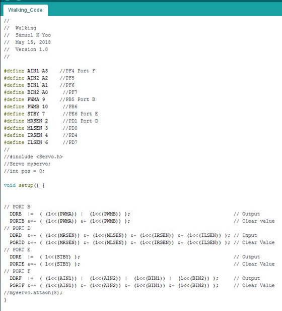
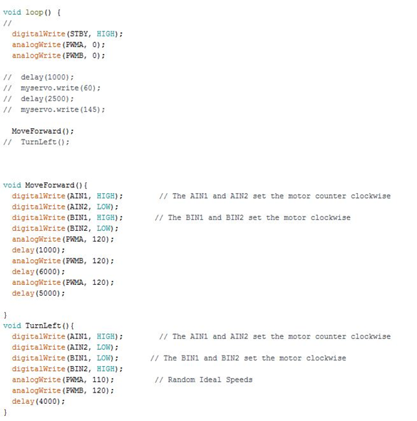
One issue identified in the system integration and assembly was the wire management and routing. As mentioned by the customer, the project should be designed from the cabling. Additional time should be spent on this section from the MST. As for testing peripherals, this should be done as soon as possible. One mistake on my part was starting late to do any testing on peripheral devices with the rest of team. For the verification document, I learned the hard way to not separate every requirement and make too many test cases. After meeting with the customer on a frequent basis, I went from 15 test cases to 8 test cases. One recommendation for future MSTs is to verify all requirements as soon as you can. Even if you do not have the 3DoT board in time, prototype with a sparkfun pro micro board. A heads up, order extra parts in case they stop working when testing is begun. Level 1 and Level 2 requirements were defined by the customer, but I recommend to meet with the customer to make sure the wording makes sense and that all system/subsystem requirements have a path back to high-level requirements. This will save you a lot of time when you are writing test cases. In my experience, all verification should be done at the Level 1 requirements. This is allowed since all system requirements lead back to Level 1 requirements.

Electronics & Control Engineer Remarks

By: Kris Osuna

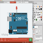
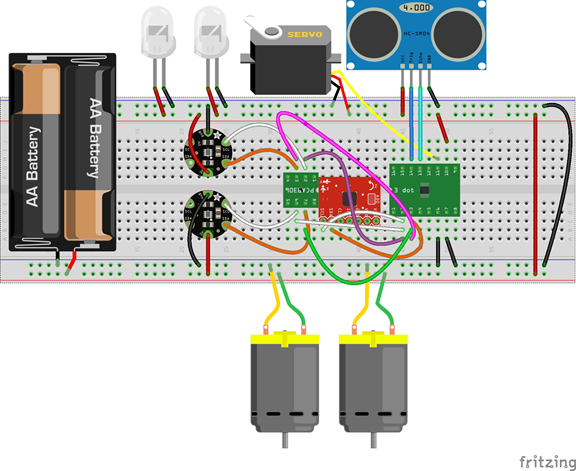
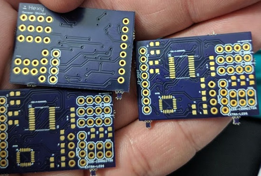
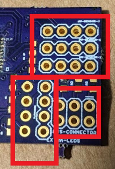
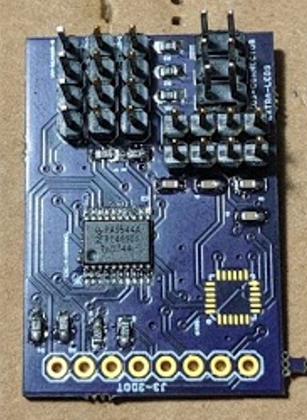
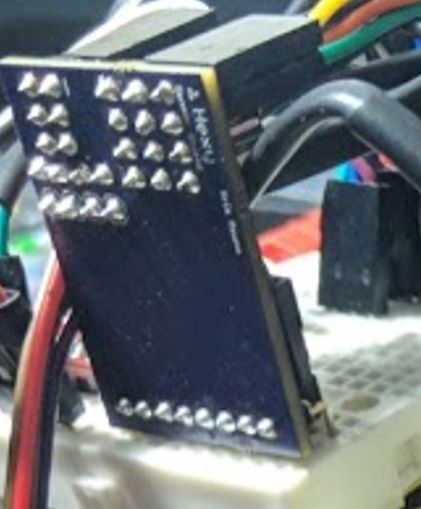
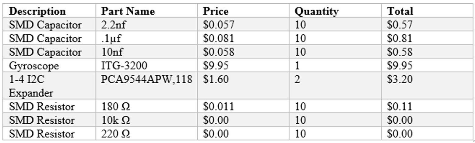
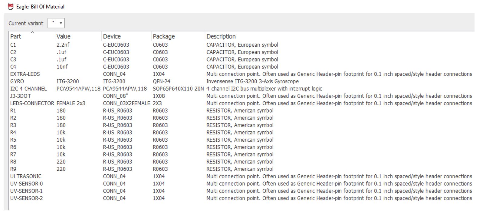
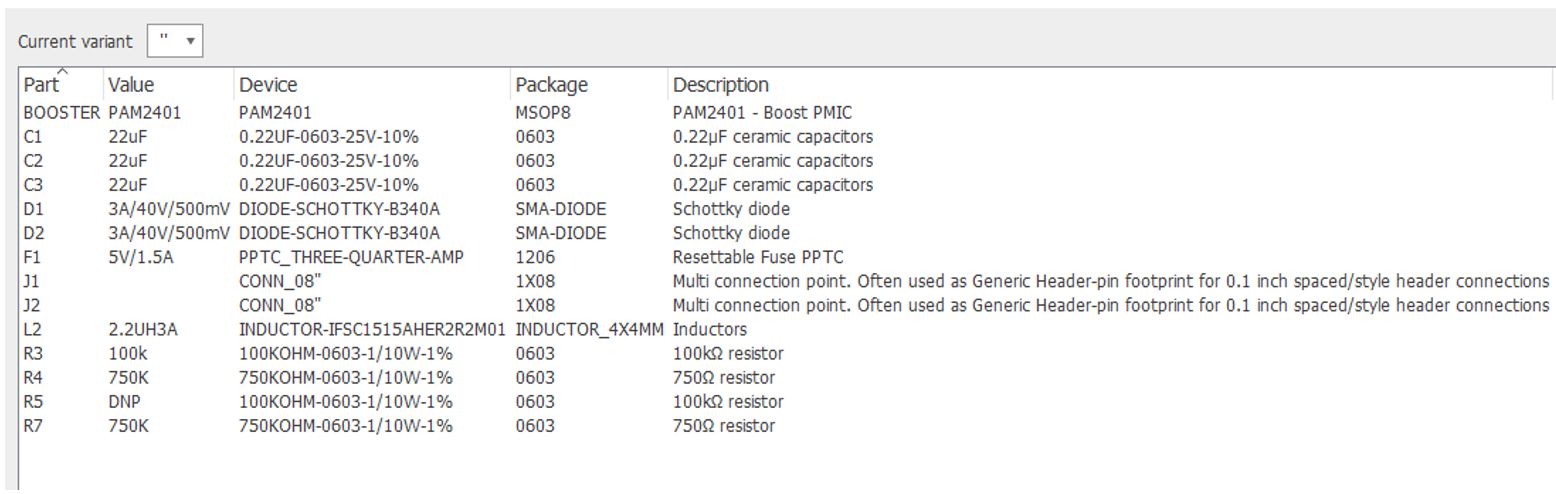
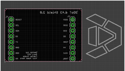
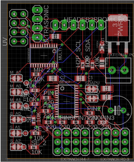
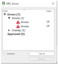
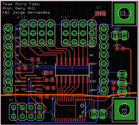
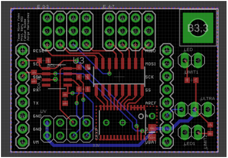
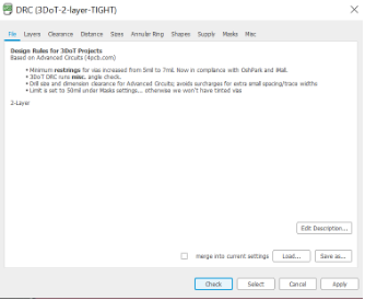
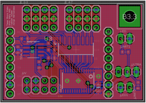
Getting familiar with Fritzing and EAGLE software is very important. Fritzing gives a visual for the end product. It shows you the pins you need and if the project is possible. I recommend working on the schematic and PCB as soon as possible. When making the schematic do not pick the first part you find in the EAGLE library. I highly suggest researching the part you are thinking about using. A mistake I made was not checking the availability of the integrated circuits I used in my schematic. The gyroscope I chose was three generations back and was unavailable in most places. The unavailability meant I could not purchase the item with the other components increasing the shipping costs and the overall cost of the project. I learned that when I finish the PCB the PCB is not done. The PCB goes through multiple levels of quality checks. If you turn in the PCB design on Monday you will get feedback and changes that need to be done, which will make your finished date Friday. Take into account corrections you might need and give yourself extra time for it. I suggest planning for redesigns and things that need to be fixed. Purchase extra pieces because things can go wrong.

Take pictures all the time. When doing blog posts I found that I was not taking enough photos to show the work being done. It is easier to show something than it is to describe something. Stay on top of your blog posts. Start your blog posts as you go along even if you do not finish because the event you are posting about just happened and it is harder to remember.

Manufacturing Engineer Remarks


By: Eduardo De La Cruz (Project Manager and Manufacturing Engineer)

Purchase a digital caliper if you do not have one already you will find it very useful throughout the semester. Learning SolidWorks as soon as possible is critical to getting things done in time. The Manufacturing Engineer should become competent in designing simple parts by the end of the first month and should be able to make more complex parts by the end of the second month. Review during every class meeting with the professor, a.k.a the customer, design changes or ideas as you will come to learn that sometimes the customer does not agree or like what you are making and will send you back to the drawing board. Sometimes groups would go weeks working on something only for the customer to dislike it and making them start over. Therefore, COMMUNICATION with the customer is critical to finishing things on schedule.


Getting acquainted with more than one 3D printing source will play to your advantage. The professor recommends his own 3D printing guy (Ridwan), however, far too often 3D prints would get delayed for days due to everyone reaching him around the same time. The manufacturing engineer should consider other 3D printing sources such as CSULB Makers group (located in VEC 518) or other off-campus printing shops.


When printing parts it is very important to consider how the part will be placed for printing. Like wood, 3D prints will have either vertical layers or horizontal layers based on the printing position. Sometimes moving parts will require you to pick a specific printing position in order to prevent layer splitting, or if you are considering inserting threaded screws into the material. If the layering is perpendicular to the angle at which the screw is being inserted you will most likely split the printing material as you insert the screw. Click here to read more about layering and print positioning.


Print positioning is also very important when it comes to parts that will be elevated off the ground at an angle greater than 45 degrees. Areas that will be off the ground will require print support in order to prevent sagging. Adding support decreases the print quality, as well as increases 3D print times. Click here to read more about this.


Finally, when talking to your 3D printing supplier, it is important to understand the role layer height plays in determining the quality and cost of the print. The thickness of each layer determines the resolution of the print. The smaller the layer height the smoother the print. However, as layer height decreases the longer the print and the higher the cost. Usually for prototyping, since time is critical to meet the 2-2-2 print requirement, layer height might be set around .3 mm for quicker production, whereas for final prints layer height could be less than .1mm since time is not an issue. Click here to read about layer heights.


References

  1. https://www.3dhubs.com/knowledge-base/how-does-part-orientation-affect-3d-print
  2. https://www.3dhubs.com/knowledge-base/supports-3d-printing-technology-overview
  3. https://support.formlabs.com/hc/en-us/articles/115000015870-When-to-Use-Different-Layer-Heights

Spring 2018 3DoT Hexy: Custom PCB Assembly

By: Kris Osuna (Electronics & Control Engineer)

Verified by: Eduardo De La Cruz (Project Manager and Manufacturing Engineer)

Approved by: Miguel Garcia (Quality Assurance)

Introduction

The custom PCB only has two IC chips. On the PCB we have the I2C expander that will read the three calibrated light sensor values and the gyroscope. The gyroscope will also be incorporated on the custom PCB and will be used to make turns. The reason only two IC chips are on the PCB is due to the location of the 3DoT in relation to where the IC chips need to be. We use headers and cables to connect from the PCB to the IC chips, specifically the three calibrated light sensors, the ultrasonic sensor, and five LEDs. The sensor shield will connect to the J3 header of the 3DoT board.

Related Requirements

Level 1 Requirements

  • The robot will need to navigate remotely through a custom-built maze (built by AoSa image), memorize the path it took, start over, and autonomously travel through the path it took.
  • The robot shall avoid collisions if it encounters other robots while navigating through the maze. This involves detecting the robot, retracing steps back, and moving to a room that allows the other robot to have a safe passage.
  • The robot shall use a v6.43 3DoT board.
  • The robot shall demonstrate the capabilities of the 3DoT micro-controller for DIY hobbyists.

Level 2 Requirements 

  • The robot shall use a single RCR123A 3.7 V, 650mA rechargeable Li-ion battery to power the 3DoT board, which will power the drivetrain and all attached peripherals.
  • The robot shall use three calibrated light sensors connected to a custom PCB.
  • The robot shall use a HC-SR04 ultrasonic sensor to handle robot avoidance.
  • Ultrasonic sensor shall have a range of 0.5-meter radius to detect and respond accordingly to other robots.

PCB Assembly

Figure 1: Sensor shield fabricated from the EAGLE schematic.

Figure 2: SMD 603 package resistor size compared to penny

Figure 3: Solder paste is spread on all SMD components

Figure 4: Placing PCB in the reflow oven. A gif can be found here.

Figure 5: Solder flowing in the reflow oven. A gif can be found here.

Figure 6: Pin headers will have to be manually soldered on

Figure 7: Finished PCB

Figure 8: Back of the PCB with all connections

Conclusion

The sensor shield could have gone on J1 and J2 and placed on top of the 3DoT but the sensor shield was designed for J3. Originally, we were going to have a booster shield on J1 and J2 so sensor shield had to go to the J3 header. Testing on the finished soldered PCB showed that only channel two on the I2C expander is getting data. I tried cleaning up the soldering on the I2C but it did not fix the problem. If we cannot get all 4 channels working a breakout board might be used. When the Gyroscope arrives we will solder the gyroscope on.

References

  1. https://www.arxterra.com/spring-2018-3dot-hexy-sensor-shield-layout/
  2. https://gfycat.com/AnimatedGeneralAcornweevil
  3. https://thumbs.gfycat.com/EnlightenedFrailHornet-size_restricted.gif

Spring 2018 3DoT Hexy: Electronic Component BOM and Order

By: Kris Osuna (Electronics and Control Engineer)

Verified by: Eduardo De La Cruz (Project Manager and Manufacturing Engineer)

Approved by: Miguel Garcia (Quality Assurance)

Introduction

The 3DoT Hexy project will be using the following electronic components.

05/08/2018

The complete cost will be $123.72 which includes shipping and handling. We will not be using the booster shield so none of the components for the booster shield were ordered. Below you can see the cost of the parts. A price of $0.00 means the parts were obtained from the resource cabinets and did not have to be purchased.

Figure 1: Purchase parts 

04/19/2018

We will be making two custom PCBs, one for the sensor and one for the booster shield to power our motors. A team member has an ultrasonic sensor so one does not need to be purchased.

Figure 2: Hexy Sensor Shield BOM

Figure 3: Booster Shield BOM 

Figure 4: Electronics that will not go on the PCB but will still be needed 

Conclusion

Electronic components will cost $108.81. This price does not include shipping and handling. When the purchase is made we will update the total. We will be ordering more parts than we need in case there is a problem soldering the components.

References

  1. EAGLE BOM Extraction

Spring 2018: BiPed Custom PCB Layout/Design & Modify Micro FOBO for 3DoT

By: Jorge Hernandez (Electronics & Control Engineer)

Verified By: Miguel Gonzalez (Project Manager)

Approved By: Miguel Garcia (Quality Assurance)

Table of Contents


Introduction

The PCB layout for Micro FOBO was modified to fit the 3DoT which will be provided by Professor Gary Hill. The way we modify Micro FOBO for a 3DoT board is by having the blank 3DoT layout template, which was kindly provided to us, and implement the pinouts in our board layout design. Once we have our template where the pins are ready to mount to the 3 DoT directly, we can start routing and building the PCB for Micro FOBO.

Given

Fig.1 3DoT 6.41 Shield

This is the blank pin headers for the 3DoT which was created by Gary Hill and Fabian Suske for the Spring 2018 semester.

Fig.2 3DoT Shield Pins

Board layout for 3 DoT pin header above with the correct dimensions, will be used as a foundation to build the PCB for Micro FOBO. This board layout was also provided by Gary Hill and Fabian Suske.

Non approved layouts

Fig.3 First Custom Shield V1

When I first started routing, it was a total mess to be honest. I had all the addresses for the servo expander & Multiplexer on the board layout which just took up a lot of space. I was also using the wrong Multiplexer as it was an 8 Channel Multiplexer which was just a huge waste of space as I only needed a 2-channel multiplexer. Another mistake I had was having everything connected to my external battery source ‘VBATT’ which is not necessary because everything but the Servo Expander operates at 3.3V just like the 3DoT. As one can see I was using the 4 pin header for the Ultrasonic(HC-SR04) which only operates at 5 V. Now using a SEEED ultrasonic, which operates at 3.3V and only has 3 pins, eliminates a need for a booster shield.  I also learned about DRC, which is “Design rule checking or check(s) (DRC). This is the area of electronic design automation that determines whether the physical layout of a particular chip layout satisfies a series of recommended parameters called “design rules” and my first board layout had many errors as seen below.

Fig.4 DRC Errors

Second draft

Fig.5 Custom Shield V2

Having 90-degree bends are not allowed and is a reason this board layout did not get approved. Another reason is how some wires were not routed to its simplest form, therefore the routing needed to be more direct. Since the plan was to mount our PCB on top of the 3DoT, everything below the orange line will interfere with the battery which will need to be moved to accommodate this issue. Also, the size of this vias needs to be increased as they are too tiny. The power routing width needs to be increased to satisfy the current running through the power routings.

Final approved Layout

Fig.6 Custom Shield Final Version

The reason this board is approved

  1. No 90-degree routes
  2. Direct/clean wiring
  3. Larger vias
  4. No battery interference
  5. Power wiring widths are larger
  6. Ratsnest and DRC were satisfied

Fig.7 DRC-All Clear

Finished routed board

Fig.8 Custom PCB Eagle

Custom Parts

The PCA9540BDPN 2-channel multiplexer default part from Digikey gave us overlapping pinouts which didn’t go through OSHParks DRC. Therefore I had to go directly to its library and move the pins apart in order to use this part.

Before the modified PCA9540BDPN chip

Fig.9 Before-PCA9540BDPN Chip

It is obvious changes needed to be done to prevent overlapping

After the modified  PCA9540BDPN chip

Fig.10 After-PCA9540BDPN Chip

Modified pins and DRC approved.

Conclusion

My Micro FOBO board layout consists of 2 UV headers, a Servo Expander, 8 micro servo pin headers, a coupling capacitor, resistors, LED pin headers, ultrasonic pin headers, and a 2 channel multiplexer. The exact specifications of these components can be found at Micro FOBO Electronics Component BOM blog post. The final PCB board layout is 39.958 x 27.941 mm which fits perfectly on top of the 3 DoT which is 60×74 mm which overall fits within Micro FOBO’s head which measures 60×74 mm.

References

  1. https://www.arxterra.com/spring-2016-rofi-pcb-layout/
  2. https://en.wikipedia.org/wiki/Design_rule_checking


Spring 2018: BiPed (Micro FOBO) System Block Diagram

By: Jorge Hernandez (Electronics & Control Engineer)

Verified By: Miguel Gonzalez (Project Manager)

Approved By: Miguel Garcia (Quality Assurance)


System Block Diagram

New and improved System Block Diagram for Micro Fobo, which shows in a general diagram, how many pins will be needed for each component and how they connect to each other.  As seen, we are using a total of 5 sensors, a custom PCB, Bluetooth module, external battery and of course a Pro Micro. This helps a lot for our E&C engineer when it comes to PCB designing as they need to plan accordingly.

Fig.1 Micro FOBO System Block Diagram

The sensors subsystem (custom PCB) will be in charge of telling Micro FOBO’s next action.  When the IR sensor on the UV breakout board sense a change in IR reading, this will alert the Pro Micro which ultimately leads to the Actuators subsystem (Micro Servos) to adapt accordingly based on our code.  The same process will occur when the Ultrasonic sensor senses an object or a wall ahead of Micro Fobo. Bluetooth is considered a sensor because it collects inputs from a source, in this case, an Android phone then sends that data to the Pro Micro thus telling Micro FOBO what to do based on our code.  The communication subsystem (Bluetooth module) is connected to the Pro Micro because through Bluetooth the Arduino will obtain information on the action it will take. The Power subsystem consists of the battery which has been tested for our overall system and a regulator to ensure the safety of the system and the user(s).  Our Actuator subsystem is our output, Micro FOBO’s desired movement, based on our sensors and code

References

  1. https://www.arxterra.com/spring-2016-rofi-preliminary-design-documentation/#System_Block_Diagram