PCB Fabrication
Author: Diane Kim (Division Manager of E&C Hardware)
Verified By: Jordan Smallwood (Project Manager)
Approved By: Miguel Garcia (Quality Assurance)
Table of Contents
Introduction
To fabricate our board, we use a PCB fabrication machine called the V-One from Voltera. Its function includes printing, soldering, and drilling.
Printing
V-One uses conductive ink to print the traces of the circuit. It will print the traces and bake it as well. The limits of the traces are:
- Minimum 8 mil trace width and spacing
- Minimum 0.65 mm pin pitch for SMT components
- Minimum 0603 passive size
- Minimum circuit size 1 x1 mm
Soldering
After the trace is done, the V-One can print the solder paste onto the desired traces. The user must manually place the pieces onto the board. After the pieces are place, the V-One will bake the board once more to heat up the solder paste. The limitations of soldering are:
- Minimum 0.5 mm pin pitch for SMT components
- Minimum 0402 passive size
Drilling
The V-One can also drill holes through the circuit board. The drill sizes are 0.7, 0.8, 0.9, 1.0, 1.6 mm for the diameter. Therefore, the smallest hole size is 0.7 mm which is 27.6 mil. To connect the top and bottom layer, rivets are used, and the given rivet sizes are 0.4 mm and 1.0 mm for the inside diameter.
Software
To communicate between Eagle CAD and the V-One, Gerber files are used. V-One has its own CAM processor that outputs the top, bottom, solder paste and drill layers. Once the Gerber files are converted from the Eagle CAD, it is uploaded into the Voltera software which allows the user to choose the desired action: print, solder, bake, or drill. Each process has its own procedure which the user can follow easily with the guidelines that are shown through the process on the right side of the window.
Procedure to Fabricate the Board
Drilling:
Drilling is done first. The board is placed onto the pad and then the drill size is chosen. For our board, we are using the 0.7 mm and the 1.6 mm drills.

Figure 1. Picture of the drill in action
Printing:
After the drilling is done, the top layer is printed first. The board is not moved therefore the previous alignment can be used. After the conductive ink is printed, the board is heated to bake the conductive ink.
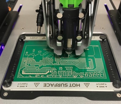
Figure 2: printing process
After the top layer is baked, the board is flipped to print the bottom layer. Since the board is moved, alignment is needed so that the top and bottom match. After the alignment is done the bottom layer is printed and baked.
Connecting Top and Bottom Layers:
The top and bottom layer are connecting using the rivets. The flat side of the rivets are placed into the through-holes connecting the top and bottom. To flatten the non-flat side of the rivets, the rivets pressing tool is used. After each rivet is pressed, the multimeter was used to confirm that there is a connection between the top and bottom pads.
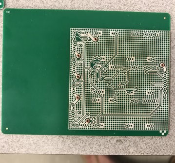
Figure 3: Rivets done
Cutting the Board
We needed to cut the board because the machine doesn’t have the function to do so. Therefore, we used the machines given access to mechanical engineering majors to do so.
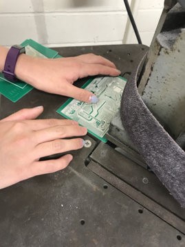
Figure 4: Cutting the excess part of the board
Soldering:
Alignment is needed once again since the board is moved so that the location of the pads is known to the machine. The solder paste is printed on the pads and the components are placed onto the correct locations and baked once more.
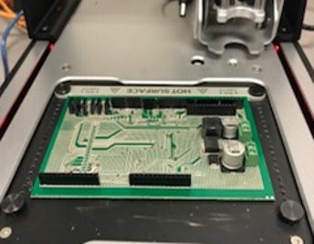
Figure 5. Picture of the soldering
After the surface-mount component is placed, the through hole components. For our board, we had male and female connectors that needed to be hand soldered. Following the guide form the soldering workshop blog post, the connectors were hand soldered
Final Testing:
The final product is shown below and the connections were checked using a multimeter. Basing off the interface matrix, the connection between the peripheral systems pinout and the ATmega2560 pinout was checked. All the connections were checked.

Figure 6: Final Project
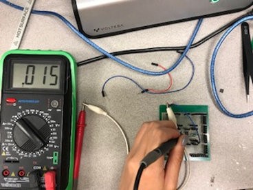
Figure 7. Testing the connection of the traces
Conclusion
The time taken to fabricate the PCB was 7 hours. It took two hours to draw the traces for each side, one hour to bake the traces, and another hour to solder on everything. When it came to testing the board, we weren’t able to due to technical problems. We were able to connect all the components onto the circuit board and the ATmega256. However, during the process, the board got shorted and damaged the board. We didn’t have enough time nor material to print out the board, therefore, we weren’t able to print out another one.
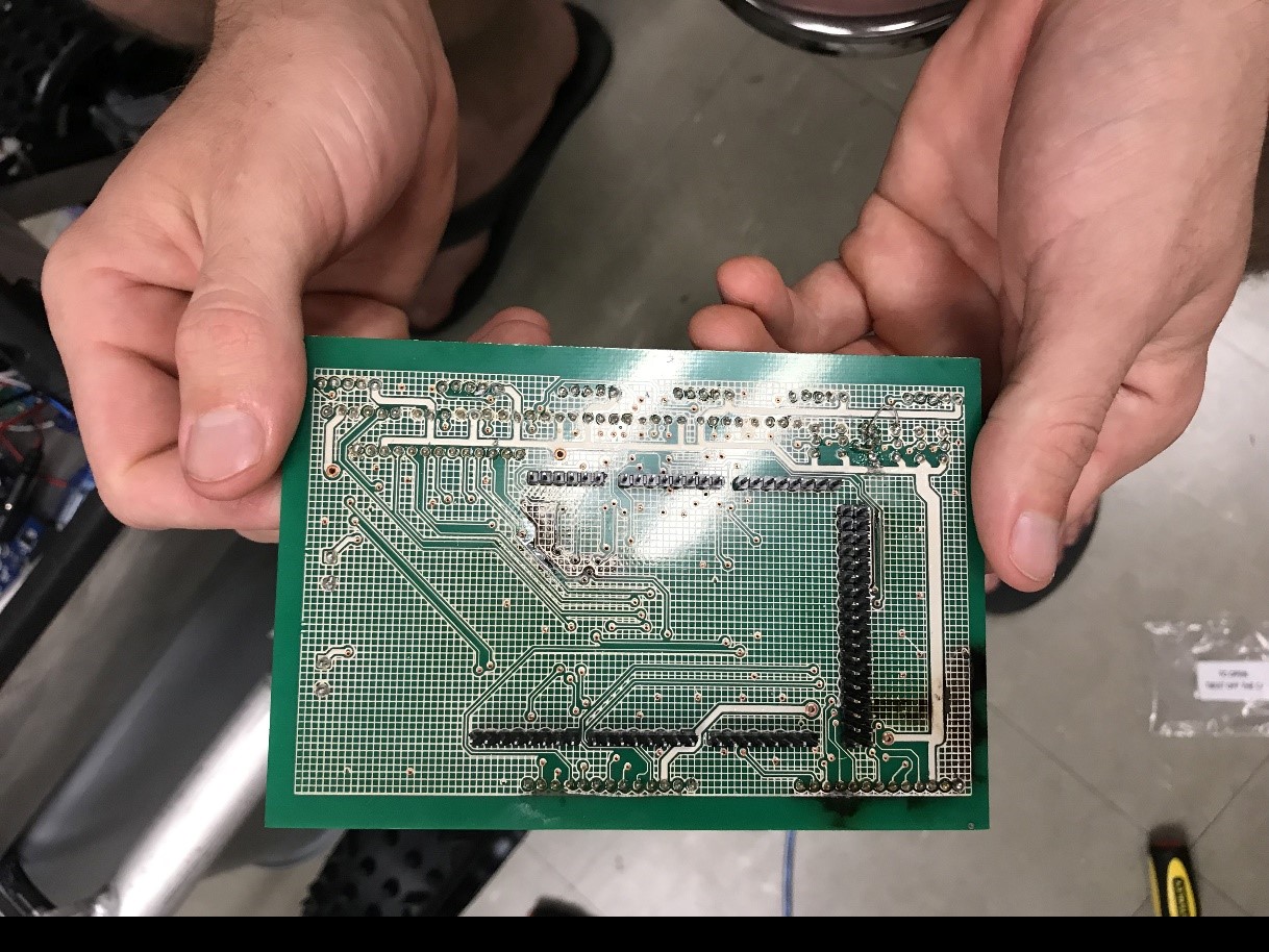
Figure 8: Image of the damaged board