Pathfinder Solar Array/ Fall / 2018
Solidworks Solar Array Design
Author/s: Eduardo Charcas
Introduction
In an attempt to improve the pathfinder solar array, the team (Eddie & David) has collaborated with Professor Hill in proposing possible solutions to a few issues to mounting the solar cells onto the aluminum panels (main, rear, and both wings). The problems with mounting the solar cells included aesthetics, amount of material being loaded, solar cell interconnections, and optimal placement for maximum quantity availability of solar cells on the panels. One possible solution to this, which is currently being pursued is to mount each solar cell onto a custom PCB by soldering. The PCB would have connectors for series or parallel connections between other solar cells. The solar cell/PCB unit would then be tightly fixed into a “H” shaped cut in the panel. The cuts are “H” shaped for the sake of having some space to work with the 4 connector pins (In/Out) and wiring.
Body
The dimensions shown below in the Solidworks images are in millimeters. The thickness of all the panels is 3.57mm.
Also, the 80mm x 55mm solar cells shall be placed where the rectangular dashed lines are in figure 2.
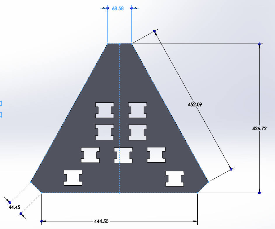
Figure 1. Main Panel with dimensions

Figure 2: Layout of the solar panels
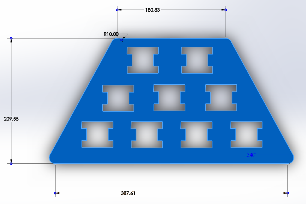
Figure 3: Rear Panel with dimensions
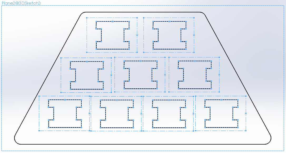
Figure 4: Rear panel with solar cell outlines and H cuts
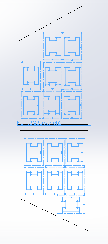
Figure 5: Side panels with solar cell outlines and H cuts
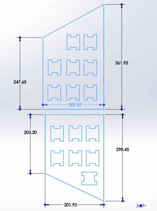
Figure 6: Dimensions of side panels
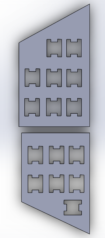
Figure 7: Solidworks model of side panels
There has been communication with the MAE shop, specifically with Mike Fritz [2] (shop technician) in an attempt to get his assistance in manufacturing these new panels out of Aluminum. Recently he has expressed concern with the amount of “H” cuts desired. He stated that because the plasma cutter is broken the only other option is to use the CNC machine. The first issue with using the CNC machine is that since the machine would need to punch a circular hole to begin cutting the pattern out, the “H” cut would not have the right angle’s depicted. Second is that each “H” cut would take half a day. Since there will be approximately 50 “H” holes to cut, this process is not feasible for the allotted time we have. So, a possible solution to this could be punching one or two circular holes large enough to mount a PCB that would still have the necessary space for the solar cell and other components where the “H” cuts are.
Conclusion
In conclusion, the Panel’s design for the solar array still needs to be finalized and where they will be manufactured is still not clear. Availability of a CNC machine has not been found and more research needs to happen.
References/Resources
- Solar Array Pictures/ Solidworks Images
- Personal communications with Mike Fritz, CSULB Department of Mechanical and Aerospace Engineering (MAE) shop manager.