The Real World of External Interrupts
Reading
The AVR Microcontroller and Embedded Systems using Assembly and C
by Muhammad Ali Mazidi, Sarmad Naimi, and Sepehr Naimi
Sections: 10.3, 10.5
Table of Contents
External Interrupts
- Review ATmega328P Interrupts Lecture Notes page 4 “Interrupt Basics”
- External Interrupts are triggered by the INT0 and INT1 pins or any of the PCINT23..0 pins
- 23 Pin Change Interrupts are mapped to the 23 General Purpose I/O Port Pins:
| Port B Group | PCINT7 (PB7) |
|
| Port C Group | PCINT14 (PC6) |
|
| Port D Group | PCINT23 (PD7) |
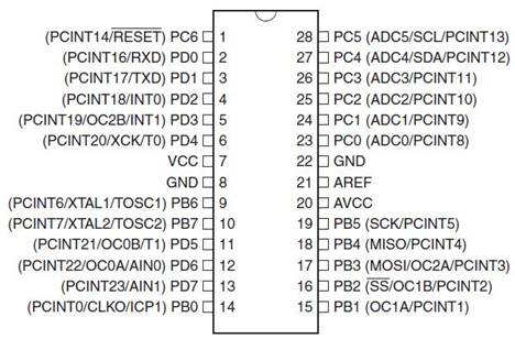
Figure 1: ATmega328P Pinout
ATmega328P Interrupt Vector Table
| Vector No | Program Address | Source | Interrupt Definition | Arduino/C++ ISR() Macro Vector Name |
|---|---|---|---|---|
| 1 | 0x0000 | RESET | Reset | |
| 2 | 0x0002 | INT0 | External Interrupt Request 0 (pin D2) | (INT0_vect) |
| 3 | 0x0004 | INT1 | External Interrupt Request 1 (pin D3) | (INT1_vect) |
| 4 | 0x0006 | PCINT0 | Pin Change Interrupt Request 0 (pins D8 to D13) | (PCINT0_vect) |
| 5 | 0x0008 | PCINT1 | Pin Change Interrupt Request 1 (pins A0 to A5) | (PCINT1_vect) |
| 6 | 0x000A | PCINT2 | Pin Change Interrupt Request 2 (pins D0 to D7) | (PCINT2_vect) |
| 7 | 0x000C | WDT | Watchdog Time-out Interrupt | (WDT_vect) |
| 8 | 0x000E | TIMER2 COMPA | Timer/Counter2 Compare Match A | (TIMER2_COMPA_vect) |
| 9 | 0x0010 | TIMER2 COMPB | Timer/Counter2 Compare Match B | (TIMER2_COMPB_vect) |
| 10 | 0x0012 | TIMER2 OVF | Timer/Counter2 Overflow | (TIMER2_OVF_vect) |
| 11 | 0x0014 | TIMER1 CAPT | Timer/Counter1 Capture Event | (TIMER1_CAPT_vect) |
| 12 | 0x0016 | TIMER1 COMPA | Timer/Counter1 Compare Match A | (TIMER1_COMPA_vect) |
| 13 | 0x0018 | TIMER1 COMPB | Timer/Counter1 Compare Match B | (TIMER1_COMPB_vect) |
| 14 | 0x001A | TIMER1 OVF | Timer/Counter1 Overflow | (TIMER1_OVF_vect) |
| 15 | 0x001C | TIMER0 COMPA | Timer/Counter0 Compare Match A | (TIMER0_COMPA_vect) |
| 16 | 0x001E | TIMER0 COMPB | Timer/Counter0 Compare Match B | (TIMER0_COMPB_vect) |
| 17 | 0x0020 | TIMER0 OVF | Timer/Counter0 Overflow | (TIMER0_OVF_vect) |
| 18 | 0x0022 | SPI, STC | SPI Serial Transfer Complete | (SPI_STC_vect) |
| 19 | 0x0024 | USART, RX | USART, Rx Complete | (USART_RX_vect) |
| 20 | 0x0026 | USART, UDRE | USART, Data Register Empty | (USART_UDRE_vect) |
| 21 | 0x0028 | USART, TX | USART, Tx Complete | (USART_TX_vect) |
| 22 | 0x002A | ADC | ADC Conversion Complete | (ADC_vect) |
| 23 | 0x002C | EE READY | EEPROM Ready | (EE_READY_vect) |
| 24 | 0x002E | ANALOG COMP | Analog Comparator | (ANALOG_COMP_vect) |
| 25 | 0x0030 | TWI | 2-wire Serial Interface | (I2C) (TWI_vect) |
| 26 | 0x0032 | SPM READY | Store Program Memory Ready | (SPM_READY_vect) |
ATmega328P External Interrupt Sense Control
- The INT0 and INT1 interrupts can be triggered by a low logic level, logic change, and a falling or rising edge.
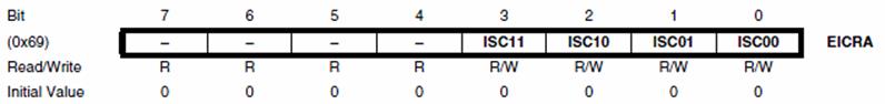
Figure 2: External Interrupt Control Register A
- This is set up as indicated in the specification for the External Interrupt Control Register A – EICRA as defined in Section 12.2.1 EICRA of the Datasheet. The number “n” can be 0 or 1.
| ISCn1 | ISCn0 | Arduino mode | Description |
|---|---|---|---|
| 0 | 0 | LOW | The low level of INTn generates an interrupt request |
| 0 | 1 | CHANGE | Any logical change on INTn generates and interrupt request |
| 1 | 0 | FALLING | The falling edge of INT0 generates an interrupt request |
| 1 | 1 | RISING | The rising edge of INT0 generates an interrupt request |
ATmega328P External Interrupt Enable
- All interrupts are assigned individual enable bits which must be written logic one together with the Global Interrupt Enable bit in the Status Register (SREG) in order to enable the interrupt.
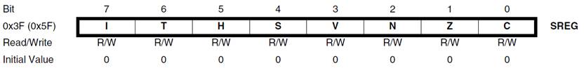
Figure 3: Status Register
- The ATmega 328P supports two external interrupts which are individually enabled by setting bits INT1 and INT0 in the External Interrupt Mask Register (Section 12.2.2 EIMSK).
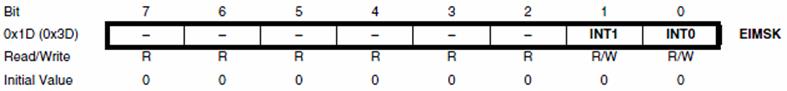
Figure 4: External Interrupt Mask Register
- Let’s look at an example. When an edge or logic change on the INT0 pin triggers an interrupt request, INTF0 becomes set (one). If the I-bit in SREG and the INT0 bit in EIMSK are set (one), the MCU will jump to the corresponding Interrupt Vector. The flag is cleared when the interrupt routine is executed.
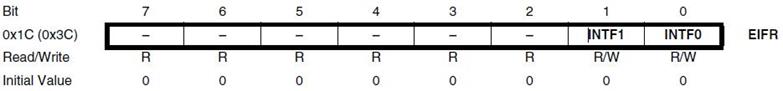
Figure 5: External Interrupt Flag Register
- Alternatively, the flag can be cleared by writing a logical one to it. The EIFR register is within the I/O address range (0x00 to 0x1F) of the Set Bit in I/O Register (SBI) Instruction. This flag is always cleared when INT0 is configured as a level interrupt.
When Will External Interrupts be Triggered?
When the INT0 or INT1 interrupts are enabled and are configured as low level triggered (Type 2), the interrupts will trigger as long as…
- The pin is held low.
- The low level is held until the completion of the currently executing instruction.
- The level is held long enough for the MCU to completely wake-up (assuming it was asleep).
– Low level interrupt on INT0 and INT1 are detected asynchronously (no clock required). The I/O clock is halted in all sleep modes except idle mode. Therefore low level interrupts can be used for waking the part from all sleep modes. - Among other applications, low level interrupts may be used to implement a handshake protocol.
When the INT0 or INT1 interrupts are enabled and are configured as edge or logic change (toggle) triggered, (Type 11) the interrupts will trigger as long as…
- The I/O clock is present.
– This implies that these interrupts cannot be used for waking up the part from sleep modes other than idle mode. - The pulse lasts longer than one I/O clock period. Shorter pulses are not guaranteed to generate an interrupt.
PIN Change Interrupts
- In addition to our two (2) external interrupts, twenty-three (23) pins can be programmed to trigger an interrupt if there pin changes state.
- These 23 pins are in turn divided into three (3) interrupt groups (PCI 2:0) corresponding to the three GPIO Ports B, C, and D
- Each of the groups are assigned to one pin change interrupt flag (PCIF) bit (2:0).
- A pin change interrupt flag will be set, if the interrupt is enabled (see How to Enable a Pin Change Interrupt), and any pin assigned to the group changes state (toggles).
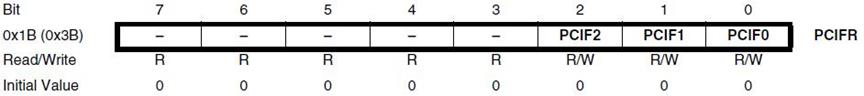
Figure 6: Pin Change Interrupt Register
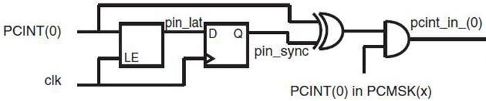
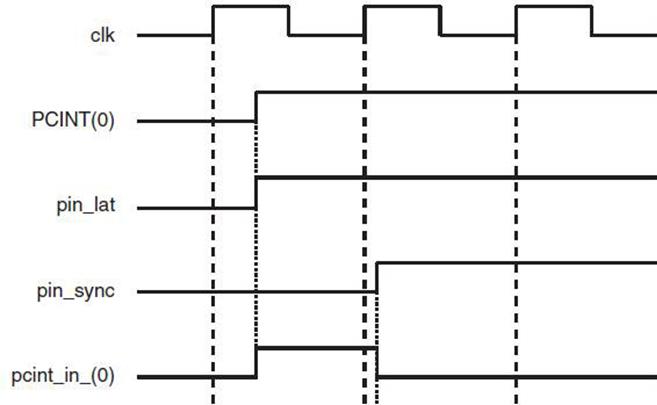
How a PIN Change Interrupt Works
Here is how it works…
How to Enable a PIN Change Interrupt
In addition to our two (2) external interrupts, twenty-three (23) pins PCINT 23:16, 14:0 can be programmed to trigger an interrupt if there pin changes state. These 23 pins are divided into three (3) interrupt groups (PCI 2:0) of eight (8), seven (7) and (8). Consequently to enable and individual pin change interrupt 3 interrupt mask bits must be set to one (1).
- The SREG global interrupt enable bit I
- The pin change interrupt enable bit (PCIE 2:0) group the pin is assigned. Specifically, a pin change interrupt PCI2 will trigger if any enabled PCINT23..16 pin toggles. A pin change interrupt PCI1 will trigger if any enabled PCINT14..8 pin toggles. A pin change interrupt PCI0 will trigger if any enabled PCINT7..0 pin toggles.
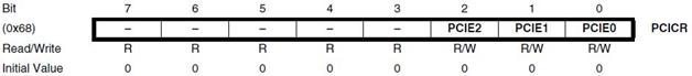
Pin Change Interrupt Control Register
- The individual pin change interrupt enable mask bit assigned to the pin (PCINT 23:0) is set. These mask bits are located in the three pin change mask registers assigned to each group.
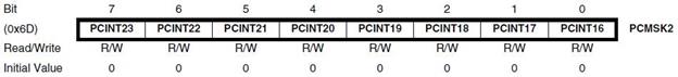
Pin Change Mask Register 2
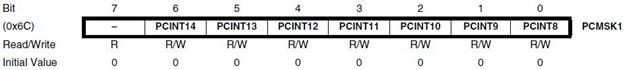
Pin Change Mask Register 1
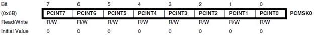
Pin Change Mask Register 0
ATmega328P Interrupt Processing (REVIEW)
Programming the Arduino to Handle External Interrupts
- Stop compiler optimization of variables within an ISR by adding the volatile qualifier. This keeps the current value in SRAM until needed.
const byte pin = 8; // green LED 0
volatile int state = LOW;
- Add jumps in the IVT to ISR routine, configure External Interrupt Control Register A (EICRA), and enable local and global Interrupt Flag Bits.
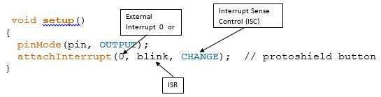
- Write Interrupt Service Routine (ISR)
void blink()
{
state = !state;
}
To disable interrupts globally (clear the I bit in SREG) call the noInterrupts() function. To once again enable interrupts (set the I bit in SREG) call the interrupts() function.
Programming the Arduino to Handle Interrupts
- In the AVR-GCC environment upon which the Arduino language is built, the interrupt vector table (IVT) is predefined to point to interrupt routines with predetermined names (see “ATmega328P Interrupt Vector Table” on page 6).
- You create an ISR by using the Macro ISR() and these names.
#include <avr/interrupt.h>
ISR(ADC_vect)
{
// user code here
}
- Now that you have defined the ISR you need to locally and globally enable it. Here are the relevant links for learning how to complete your ISR definition.
- Global manipulation of the interrupt flag
- Gammon Software Solutions forum – Interrupts
- ISR() macro
Practice Problems
Design Example – Switch Debounce
- When you press a button, its contacts will open and close many times before they finally stay in position. This is known as contact bounce.
- Depending on the switch construction, this mechanical contact bounce can last up to 10 or 20 milliseconds. This isn’t a problem for lamps, doorbells and audio circuits, but it will play havoc to with our edge-triggered interrupt circuitry.
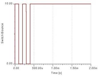
Switch Bounce
- With respect to the waveform above, a switch debounce solution must be designed to filter out these transitions.
Switch Debounce Solutions
So how can we design a “Debounce Circuit” to filter out these transitions.
- The lowest-cost solution requires no hardware. Specifically, we disable the external interrupt during the switch bounce time. This solution has been implemented for the Arduino by Nick Gammon with Arduino code provided here in the “Example code of a pump timer” section.
- For some simple electrical solutions visit http://www.patchn.com/Debounce.htm.
- For our solution, I added a D flip-flop which is clocked at a frequency less than 50 Hz (Tp = 20 milliseconds). This digital circuit acts as a low pass filter blocking the AVR interrupt circuitry from responding to any of these additional edges.
Switch Debounce Circuit – a Simple Digital Low Pass Filter
[expand title=”Appendix” tag=”h3″]
How I Designed the Debounce Circuit
Here is a real world problem that I considered while designing my Debounce circuit.
Logic Levels
Between logic 0 and logic 1 there is an undefined region . The figure below shows TTL input and output voltage levels corresponding to logic 1 and 0 (source: Theory of TTL Logic Family).
Recommended Reading: Logic signal voltage levels
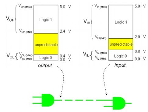
Logic Levels Based on Voltage Signal
Rise and Fall Times (Slew Rate)
Electrical signals have a finite period to transition through this region, technically known at rise and fall times or slew rate.
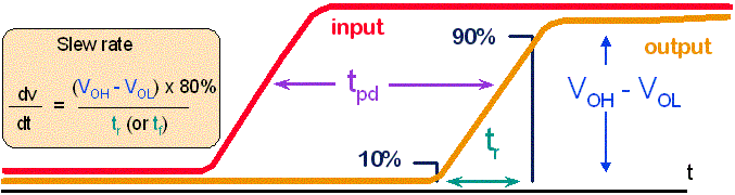
Slew Rate Graph
The table below provides data for propagation delay and slew rate for each of the families listed. Don’t allow digital logic slew rates to be slower than what is specified by the data sheet. All digital logic families will oscillate with slow rise times.
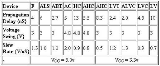
Propagation Delay & Slew Rate for Each Digital Logic Family
For some micro-controller inputs rise and fall times can be no more than 20 nsec. If this specification is violated the input may start to oscillate causing havoc within the device and ultimately destroying the input gate structure of the receiving gate.
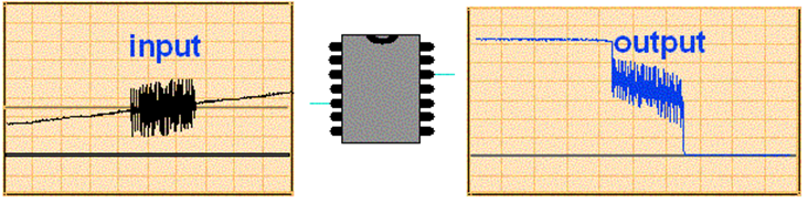
Output Distorted due to Lower Slew Rate
The input circuits of MOS devices, like our AVR micro-controller, can be characterized as capacitive in nature (can be modeled to the first order by a capacitor). For some inputs this capacitance can be as great as 10 pF (pico = 10-12). Now, let us assume an external pull-up resistor of 10 KΩ. Given this information we come up with a “back of the envelope” calculated time constant (RC) of 100 nsec.
Clearly, we have a problem. I solved this problem by adding a TTL device between the switch and the micro-controller. The input of the 74ALS74 can be characterized as resistive in nature (can be modeled by a resistor). Combined with a pull-up resistance (10 KΩ) the input problem is ameliorated.
The output of the 74ALS74 TTL device goes directly to the input of the AVR micro-controller solving our slew rate problem. This new faster circuit however introduces its own problems as discussed in the next section.
[/expand]