AVR Instruction Set Encoding
Reading
“AVR Instruction Set,” Section 6.4 “General Purpose Register File,” and Section 7.3 “SRAM Data Memory” in document doc0856 “The Program and Data Addressing Modes.”
Table of Contents
Instruction Set Mapping
The Instruction Set of our AVR processor can be functionally divided (or classified) into: Data Transfer Instructions, Arithmetic and Logic Instructions, Bit and Bit-Test Instructions, Control Transfer (Branch) Instructions, and MCU Control Instructions.
While this functional division helps you quickly find the instruction you need when you are writing a program; it does not reflect how the designers of the AVR processor mapped an assembly instruction into a 16-bit machine instruction. For this task a better way to look at the instructions is from the perspective of their addressing mode. We will divide AVR instructions into the following addressing mode types.
Data Addressing Modes
- Direct Register Addressing, Single Register
- Direct Register Addressing, Two 32 General Purpose Registers Rd and Rr
- Direct Register Addressing, Two 16 and 8 General Purpose Registers Rd and Rr
- Direct I/O Addressing (including SREG)
- Direct I/O Addressing, First 32 I/O Registers
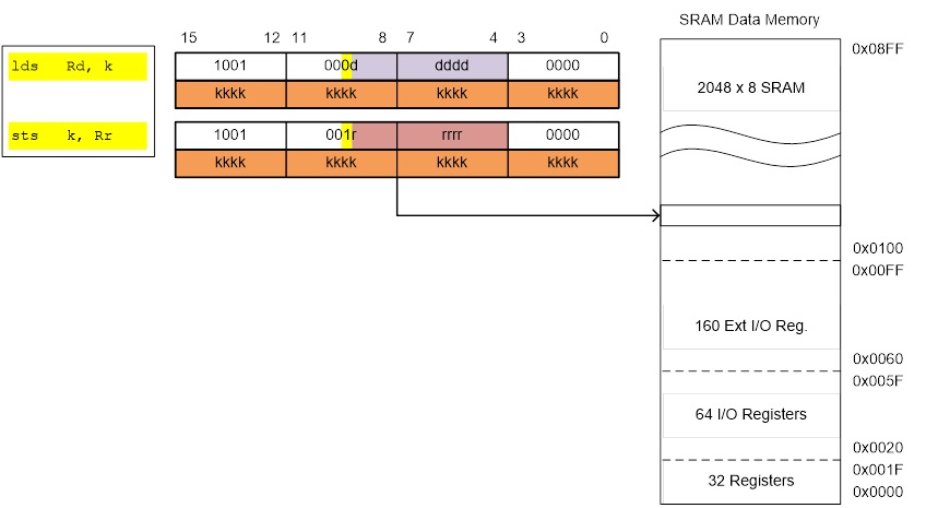
- Direct SRAM Data Addressing
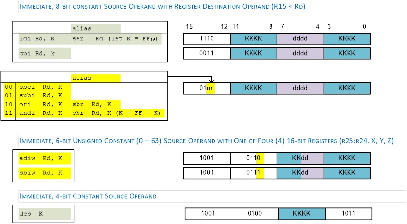
- Immediate 8-bit Constant
- Immediate 6-bit and 4-bit Constant
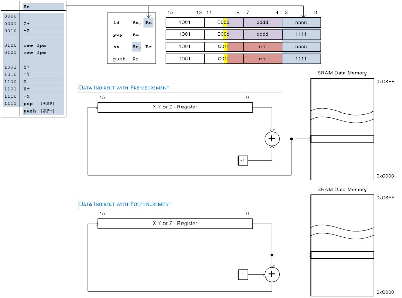
- Indirect SRAM Data Addressing with Pre-decrement and Post-increment
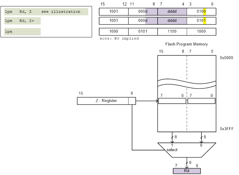
- Indirect Program Memory Addressing (Atmel Program Memory Constant Addressing)
Control Transfer
- Direct
- Relative, Unconditional
- Relative, Conditional
- Indirect
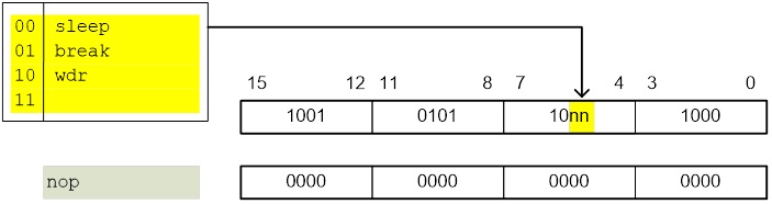
MCU Control Instructions
ATmega328P Operand Locations
When selecting an addressing mode you should ask yourself where the operand is (data) located within the AVR processor.
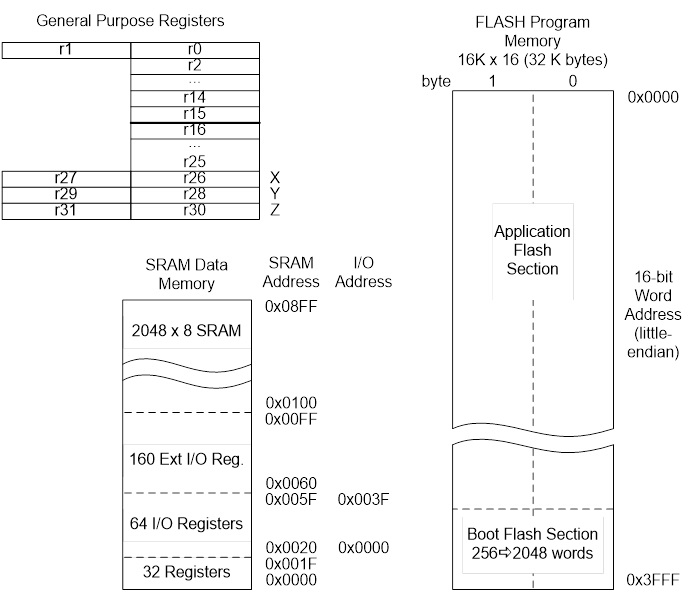
DATA ADDRESSING MODES
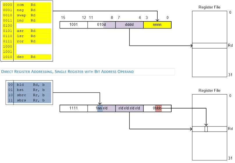
DIRECT REGISTER ADDRESSING, SINGLE REGISTER
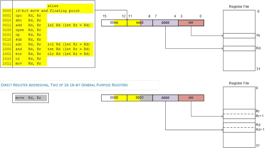
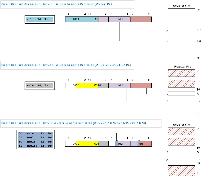
DIRECT REGISTER ADDRESSING, TWO OF 32 8-BIT GENERAL PURPOSE REGISTERS RD AND RR
Multiply
DIRECT I/O ADDRESSING (INCLUDING SREG)

DIRECT SRAM DATA ADDRESSING
IMMEDIATE
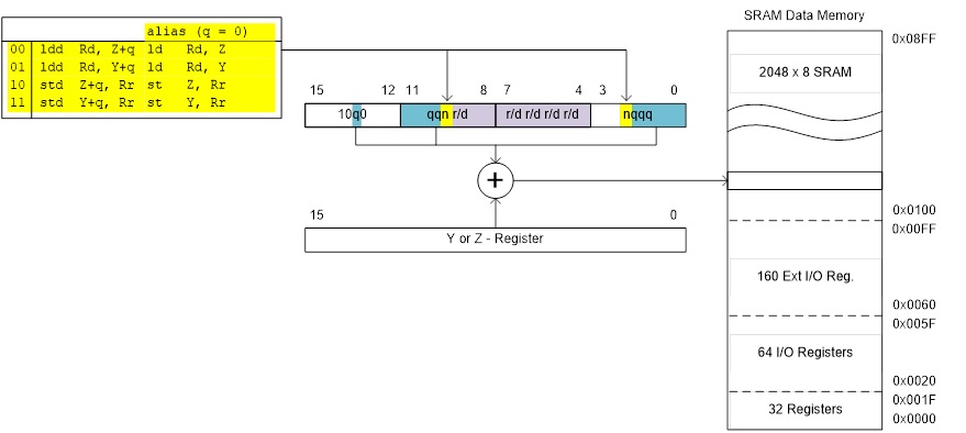
INDIRECT SRAM DATA WITH DISPLACEMENT
INDIRECT SRAM DATA ADDRESSING WITH PRE-DECREMENT AND POST-INCREMENT
INDIRECT PROGRAM MEMORY ADDRESSING (ATMEL PROGRAM MEMORY CONSTANT ADDRESSING)
CONTROL TRANSFER
DIRECT
All control transfer addressing modes modify the program counter.
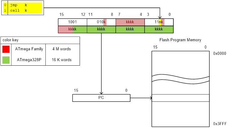
Figure 11: JMP & CALL Machine Code Stored in Flash Program Memory
INDIRECT
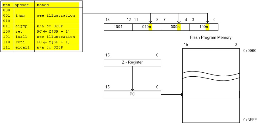
Figure 12: Indirect Instructions Machine Code
RELATIVE
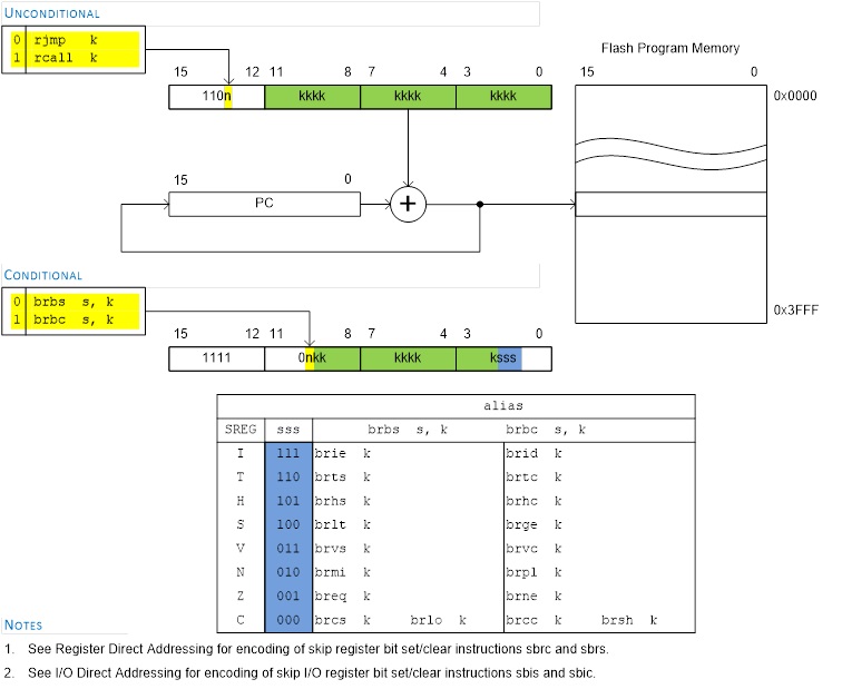
Figure 13: Relative Branching Machine Code Stored in Flash Program Memory
MCU CONTROL INSTRUCTIONS
PROGRAM DECODING – WHO AM I?
Addr Machine Instruction
Who_Am_I #1:
0204 9a5d ____ ____, ____ // I/O direct
0205 985d ____ ____, ____ // I/O direct
0206 9508 ____
[expand title=”Solution”]
pulse: ← Who Am I #1
0204 9a5d sbi PORTD,dff_clk // Set clock (2 clock cycles)
0205 985d cbi PORTD,dff_clk // Clear clock (2 clock cycles)
0206 9508 ret
[/expand]
Who_Am_I #2:
01f8 934f ____ ____ // Indirect SRAM Data Addressing
01f9 b74f ____ ____, ____ // I/O Direct
01fa 930f ____ ____ // Indirect SRAM Data Addressing
01fb 9180 0103 ____ ____, ____ // Direct SRAM Data Addressing
01fd 9100 0102 ____ ____, ____ // Direct SRAM Data Addressing
01ff 2380 ____ ____, ____ // Direct Register Addressing,
0200 910f ____ ____ // Indirect SRAM Data Addressing
0201 bf4f ____ ____, ____ // I/O Direct
0202 914f ____ ____ // Indirect SRAM Data Addressing
0203 9508 ____
[expand title=”Solution”]
hitWall: ← Who Am I #2
01f8 934f push reg_F // push any flags or registers modified
01f9 b74f in reg_F,SREG
01fa 930f push work0
01fb 9180 0103 lds cppReg,imageD
01fd 9100 0102 lds work0,imageR
01ff 2380 and cppReg,work0
0200 910f pop work0 // pop any flags or registers placed on the stack
0201 bf4f out SREG, reg_F
0202 914f pop reg_F
0203 9508 ret
[/expand]
PROGRAM ENCODING – DISPLAY
display:
:
_________ lds work0, imageR
_________ lds spi7SEG, imageD
_________ or spi7SEG, work0
_________ call spiTx
:
_________ ret
[expand title=”Solution”]
display:
019a 934f push reg_F
019b b74f in reg_F,SREG
019c 930f push work0
019d 9100 0102 lds work0,imageR
019f 9080 0103 lds spi7SEG,imageD
01a1 2a80 or spi7SEG,work0
01a2 940e 0109 call spiTx
01a4 910f pop work0
01a5 bf4f out SREG,reg_F
01a6 914f pop reg_F
01a7 9508 ret
[/expand]
PROGRAM ENCODING – TURN LEFT
; ————————–
; ——- Turn Left ——–
turnLeft:
_________ push reg_F
_________ in reg_F,SREG
:
_________ lds work0, dir // x = work0 bit 1, y = work0 bit 0
_________ bst work0,0 // store y into T
_________ bld work1,1 // load dir.1 from T (dir.1 = y)
_________ com work0 // store /x into T
_________ bst work0,1
_________ bld work1,0 // load dir.0 from T (dir.0 = /x)
_________ sts dir, work1
:
_________ out SREG, reg_F
_________ pop reg_F
_________ ret
[expand title=”Solution”]
turnLeft:
01b9 934f push reg_F
01ba b74f in reg_F,SREG
01bb 930f push work0
01bc 931f push work1
01bd 9100 0100 lds work0, dir // x = work0 bit 1, y = work0 bit 0
01bf fb00 bst work0,0 // store y into T
01c0 f911 bld work1,1 // load dir.1 from T (dir.1 = y)
01c1 9500 com work0 // store /x into T
01c2 fb01 bst work0,1
01c3 f910 bld work1,0 // load dir.0 from T (dir.0 = /x)
01c4 9310 0100 sts dir, work1
01c6 911f pop work1
01c7 910f pop work0
01c8 bf4f out SREG, reg_F
01c9 914f pop reg_F
01ca 9508 ret
[/expand]
PROGRAM ENCODING – IN FOREST AND SPITXWAIT
inForest:
Address Machine Instruction
0131 _____ ldi ZL,low(table<<1) // load address of look-up
:
02e8 _____ lds work0, row // SRAM row address = 0101
02e9
02ea _____ cpi work0, 0xFF
02eb _____ breq yes
02ec _____ clr cppReg // Compare to eor cppReg, cppReg
02ed _____ rjmp endForest
yes:
02ee _____ ser cppReg // compare to ldi cppReg, 0xFF
endForest:
:
02f3 _____ ret
[expand title=”Solution”]
inForest:
02e5 92ff push reg_F // push any flags or registers modified
02e6 b6ff in reg_F,SREG
02e7 930f push work0
02e8 9100 0101 lds work0,row
02ea 3f0f cpi work0,0xFF
02eb f011 breq yes
02ec 2788 clr cppReg // no
02ed c001 rjmp endForest
yes:
02ee ef8f ser cppReg
endForest:
02ef 2799 clr r25 // zero-extended to 16-bits for C++ call
02f0 910f pop work0 // pop any flags or registers placed on the stack
02f1 beff out SREG,reg_F
02f2 90ff pop reg_F
02f3 9508 ret
[/expand]
spiTxWait:
0112 _____ in work0,SPSR
0113 _____ bst work0,SPIF
0114 _____ brtc spiTxWait
0115 _____ ret
[expand title=”Solution”]
spiTxWait:
; Wait for transmission complete
0112 b50d in r16,SPSR
0113 fb07 bst r16,SPIF
0114 f7ee brtc spiTxWait
0115 9508 ret
[/expand]
PROGRAM ENCODING – BCD TO 7-SEGMENT DISPLAY
- Program Memory Indirect is great for implementing look-up tables located in Flash program memory – including decoders (gray code → binary, hex → seven segment, …)
- In this example I build a 7-segment decoder in software.
BCD_to_7SEG:
Address Machine Instruction
0131 _____ ldi ZL,low(table<<1) // load address of look-up
0132 _____ ldi ZH,high(table<<1)
0133 _____ clr r1
0134 _____ add ZL, r16
0135 _____ adc ZH, r1
0136 _____ lpm spi7SEG, Z
0137 _____ ret
0138 _____ table: DB 0b01111110, 0b0110000, 0b1101101 …
[expand title=”Solution”]
BCD_to_7SEG:
0131 e7e0 ldi ZL,low(table<<1) // load address of look-up
0132 e0f2 ldi ZH,high(table<<1)
0133 2411 clr r1
0134 0fe0 add ZL, r16
0135 1df1 adc ZH, r1
0136 9084 lpm spi7SEG, Z
0137 9508 ret
0138 307e
0139 6d6d table: .DB 0b01111110, 0b0110000, 0b1101101, 0b1101101
[/expand]
PROGRAM DECODING – SRAM INDIRECT
- Write and encode a program to set to ASCII Space Character (0x20), all the bytes in a 64-byte Buffer.
[expand title=”Appendix” tag=”h3″]
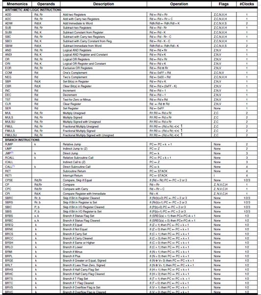
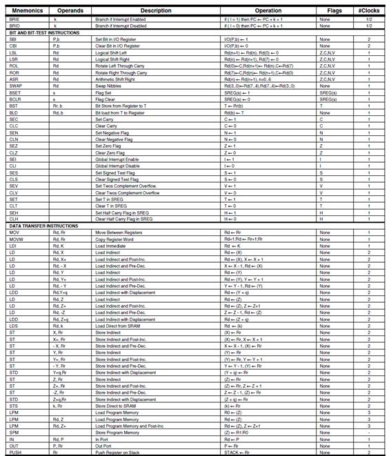
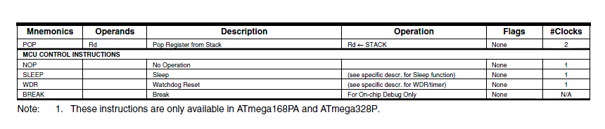
APPENDIX A: ATMEGA328P INSTRUCTION SET
APPENDIX B: ARDUINO PROTO-SHIELD SCHEMATIC
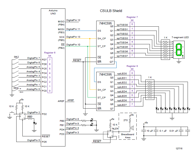
CSULB Shield
[/expand]