AVR Control Transfer: Looping
READING
The AVR Microcontroller and Embedded Systems using Assembly and C
by Muhammad Ali Mazidi, Sarmad Naimi, and Sepehr Naimi
Sections: 3.1, 3.3
ADDITIONAL READING
Introduction to AVR assembler programming for beginners, controlling sequential execution of the program http://www.avr-asm-tutorial.net/avr_en/beginner/JUMP.html
AVR Assembler User Guide
Table of Contents
LOOP CONSTRUCTS IN C++ AND ASSEMBLY
Loop Example 1: Loop through a block of code 7 times.
- Typically we increment the counter variable in C++.
for(int i=0; i<7; i++); // This statement loops 7 times {i: 0,1,2,3,4,5,6}
- As shown in the example at the right below, in assembly we decrement the counter variable.
{i: 7,6,5,4,3,2,1}
This allows us to immediately test the SREG Z-flag bit without an intermediate compare instruction.
| C++ | Assembly | |
| for(int i=7; i>0; i—-) { Block of code }
|
int i = 7; do { Block of code i—-; } while(i>0);
|
ldi r16, 7 loop: Block of code
|
BUTTON DEBOUNCE EXAMPLE
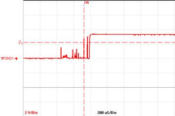
Figure 1: Debounce Timeline Source: http://generichid.sourceforge.net/buttonbounceDSO.png
- In the screen capture (red waveform), a button bounces for about 400us when pressed. Once the transition is detected, we want to design a software loop that will do nothing while the switch input stabilizes.
- Specifically, we want to design a software delay routine that will generate a delay of approx.
.
DELAY CALCULATION FOR AVR
We begin by designing a simple loop.
wait:
ldi r16, ____ // Loop Count
delay:
dec r16 // ____ machine cycles
brne delay // ____ machine cycles
To discover the delay generated by our “software” loop we begin by finding the answers to the questions.
- What “Loop Count” Lcnt will generate the maximum delay?
- What is a machine cycle and how many machine cycles are required for each line of code?
- What is the number of machine cycles Nmc in 1 loop?
INSTRUCTION (OR MACHINE) CYCLE TIME FOR THE AVR
- Machine Cycle – The number of clock cycles it takes the CPU to fetch and execute an instruction.
- Because the AVR processors incorporate a 2-stage pipeline, there is a one-to-one relationship between an AVR machine cycle and a clock cycle. In contrast for the non-pipelined 8051 microcontroller one machine cycle = 12 clock cycles.
- Therefore to calculate the time it takes for one machine cycle you only need to take the inverse of the clock frequency.
| Example: |
- As shown in the “Complete Instruction Set Summary” on page 427 of the AVR Instruction Set Document (Atmel doc0856) most AVR instructions need only one or two clock cycles to fetch and execute an instruction.

- Given a clock frequency of 16 MHz and based on the above table a multiple MUL instruction will take
to execute
- For branch instructions, the answer is not so straight forward.

PIPELINING
Before you can fully understand branching and looping you need to understand the concept of pipelining and how it is implemented in our AVR processor.
- Pipelining is a technique that breaks operations, such as instruction processing (fetch and execute) into smaller distinct stages so that a subsequent operation can begin before the previous one has completed.
- For most instructions, especially one based on a modified Harvard memory model, program memory is not accessed during the execution cycle. This memory down time could be used to fetch the next instruction to be executed, in parallel with the execution cycle of the current instruction. Here then is an opportunity for pipelining!

AVR INTERSTAGE PIPELINE REGISTERS
- A pipeline stage begins and ends with a register; controlled by a clock. Technically these are known as interstage pipeline registers.
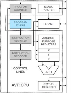
- With respect to our AVR architecture the two registers of interest are the Program Counter (PC) and the Instruction Register (IR).
- Between the register(s) is combinational logic. Although counter-intuitive, Flash Program memory can be viewed as combinational logic with an address generating a word of data.
- Without pipelining these two registers in the control unit (PC, IR) would require two clock cycles to complete a basic computer operation cycle. Specifically, an instruction is (1) fetched and then (2) executed.
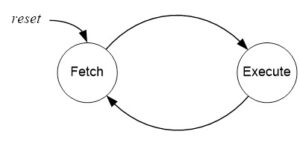
AVR TWO-STAGE INSTRUCTION PIPELINE
- The AVR pipeline has two independent stages. The first stage fetches an instruction and places it in the Instruction Register (IR), while the second stage is executing the instruction.
Figure 6: Fetch and Execute Cycle of the Atmel ATmega Microcontroller
- For our RISC architecture most instructions are executed in a single cycle (also known as elemental instructions). In this perfect world where all instructions take one cycle to fetch and one cycle to execute, after an initial delay of one cycle to fill the pipeline, known as latency, each instruction will take only one cycle to complete.
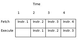
Figure 7: Program Execution in an AVR RISC two-Stage Instruction Pipelined Architecture
BRANCH PENALTY
- Within the context of pipeline architecture, when the execution stage of the pipeline is executing a conditional branch instruction, the execution stage must “predict” the outcome of the instruction in order to fetch what it “guesses” will be the next instruction.
- While on average 80% of the time a branch is taken, the AVR always guesses that the branch will not be taken. This guess is made simply because it is the simplest to implement (the program counter automatically points at the next instruction to be executed).
- When a branch is taken, and the guess is wrong, the processor must build the pipeline from scratch thus accruing a “penalty.” With our simple 2-stage pipeline that penalty is one clock cycle as shown in the AVR Instruction Set Document.
BUTTON DEBOUNCE EXAMPLE – CONTINUED
In the screen capture (red waveform), a button bounces for about 400us when pressed. Once the transition is detected, we want to design a software loop that will do nothing while the switch input stabilizes. To remove the noise, we will design a software delay routine that will generate a delay of approx. 500 us.
DELAY CALCULATION FOR AVR
- Returning to our simple software loop
wait:
ldi r16, ____ // Loop Count
delay:
dec r16 // 1 clock cycle
brne delay // + 2 cycles if true, 1 cycle if false
= Delay generated by the loop
= period of one machine cycle =
(note: 1 machine cycle = 1 clock cycle) = 1 / 16 MHz = 0.0625 usec
= number of machine cycles in 1 loop = 3 (for brne Nmc = 2 cycles, we subtract 1 for the one cases where our guess is correct.)
= number of times loop is run (Loop Count) = ?
CALCULATING MAXIMUM DELAY
- Next we will calculate the maximum delay
= 0 which results in a count of 256
(approx) Note: the -1 is subtracting the one true result
- Now Let’s increase this delay by adding a nop instruction and then recalculating the maximum delay
= number of machine cycles in 1 loop = 4
wait:
clr r16 // 0 = maximum delay
delay:
nop // 1
dec r16 // 1 clock cycle
brne delay // + 2 cycles if true, 1 cycle if false
(approx) with r16 = 0 (clr r16)
CALCULATING LOOP COUNT FOR A GIVEN DELAY
- To generate a delay of 500 µs we will initialize r16 for a delay of 50 µs and then write an outside loop that will run the inside loop 10 times for a total delay of approximately 500 µs
- Solving our Tmax equation for Loop Count Lcnt
- Set Lcnt for a delay of 50 µsec
wait:
ldi r16, 0xC8 // 200
delay:
nop // 1
dec r16 // 1 clock cycle
brne delay // + 2 cycles if true, 1 cycle if false
LOOP INSIDE A LOOP DELAY
On your own, create an outside loop with a count of 10 to give us a delay of approximately 500 µsec (Hint see Example 3-18 in your textbook)
DESIGN EXAMPLE WITH EE346 SHIELD
When the user presses the button, read first 3 switches (least significant), if the number is less than or equal to 5 then calculate factorial. If greater than 5 turn on decimal point. Display the least significant 4 bits of the answer.
MY DESIGN STEPS
Step 1: Initialized Ports
Step 2: Turned on LED 0 to indicate initialization complete
Step 3: Wrote code to pulse the clock
Step 4: Read in pin waiting for button to be pressed (Loop Example 1)
Step 5: Need to filter out Bounce (Loop Example 2)
Maximum delay that could be generated was only 48 usec
Step 6: Added a NOP instruction, max delay was now 64 usec
Set delay for nice even number of 50 usec
Step 7: Made an outside loop of 10 (Loop Example 3)
Step 8: Converted loop to a subroutine so I could change condition to button release.
Step 9: Check for button pressed and then released
Step 10: Read Switch and check if less than or equal to 6
Step 11: Calculate Factorial (Loop Example 4)
Step 12: Store 4 digit answer to SRAM (SRAM Indirect Addressing Mode)
Step 13: Sequentially, Load each digit and … (SRAM Indirect Addressing Mode)
Step 14: convert to 7-segment display (Flash Program Indirect Addressing Mode)
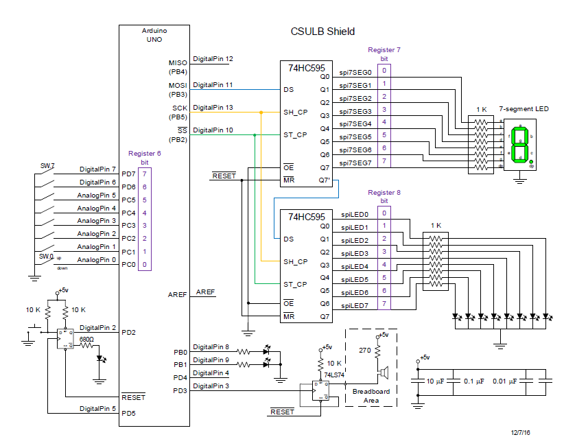
CSULB PROTO-SHIELD SCHEMATIC
CONFIGURE GPIO PORTS
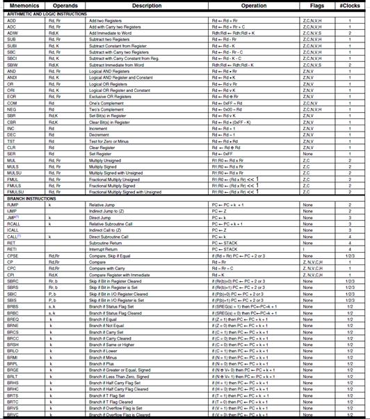
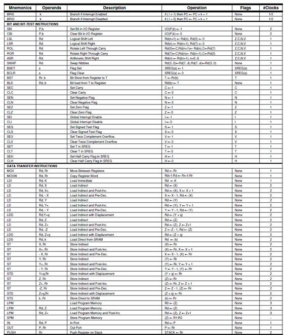
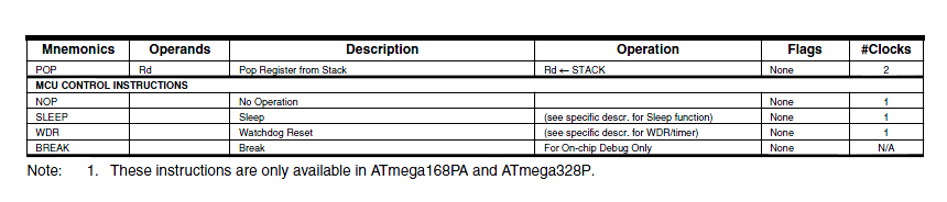
ATMEGA328P INSTRUCTION SET