General Purpose I/O Ports
Table of Contents
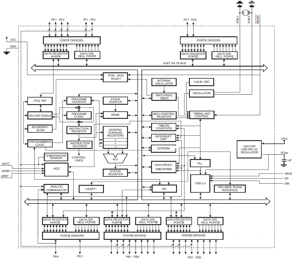
Figure 1. ATmega32U4 Block Diagram
Source: ATmega328P Data Sheet http://www.atmel.com/dyn/resources/prod_documents/8161S.pdf page 5
ATMEGA GENERAL PURPOSE DIGITAL I/O PORTS
Reading: Section 6.1.1 Introduction
- The ATmega32U4 has 26 General Purpose Digital I/O Pins assigned to 5 Ports (8-bit Ports B, D, 2-bit Port C,E, and 6-bit Port F)
- Each I/O port pin may be configured as an output with symmetrical drive characteristics. Each pin driver is strong enough (20 mA) to drive LED displays directly.
- Each I/O port pin may be configured as an input with or without a pull-up resistor. The values for the pull up resistor can range from 20 – 50 K ohms.
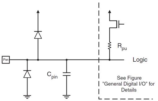
- Each I/O pin has protection diodes to both VCC and Ground
PIN DESCRIPTION OF THE ATMEGA32U4
Reading: Section 6.1.3 Pin-Muxing
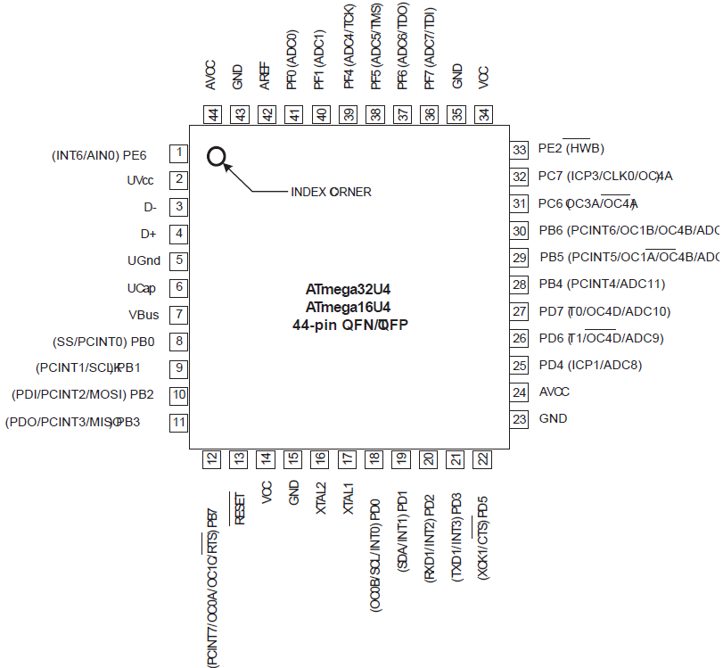
Figure 1. ATmega32U4 Pinout
I/O Ports B, C, D, E, and F
Ports B (PB7..PB0), C (PC7,PC6), D (PD7..PD0), E (PE6,PE2), F (PF7..PF4,PF1,PF0) are bi-directional I/O ports with internal pull-up resistors (selected for each bit). The Port output buffers have symmetrical drive characteristics with both high sink and source capability.
Interrupts
External Interrupts are triggered by the INT0 to INT3 and INT6 pins or any of the PCINT7..0 pins associated with Port B. Observe that, if enabled, the interrupts will trigger even if the pins are configured as outputs. This feature provides a way of generating a software interrupt.
Analog Voltage (AVCC)
AVCC is the supply voltage pin for the A/D Converter. It should be externally connected to VCC. If the ADC is used, it should be connected to VCC through a low-pass filter.
Analog Reference (AREF)
AREF is the analog reference pin for the A/D Converter.
Analog to Digital Converter (ADC)
The ATmega32U4 includes a 10-bit ADC. The ADC is connected to a analog multiplexer with six single-ended voltage input (ADC0, ADC1, ADC4 to ADC7) channels. The device also supports differential inputs, with the positive input terminal selectable between ADC4 to ADC7, and negative input terminal selectable between ADC0 and ADC1. The output of the differential amplifier goes to a gain stage, with four (4) programmable amplification steps of 0 dB (1x), 10 dB (10x), 16dB (40x), and 23dB (200x). If 1x, 10x, or 40x gain is used, 8-bit resolution can be expected. If 200x gain is used, 7-bit resolution can be expected.
I/O PORT PIN AS AN OUTPUT
Reading: Section 6.1.2 Basic Operation
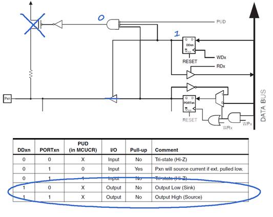
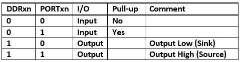
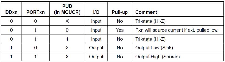
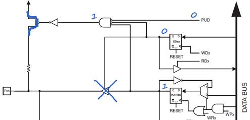
- To configure a Port (x) pin as an output set corresponding bit (n) in the Data Direction Register (DDxn) to 1. Once configured as an output pin, you control the state of the pin (1 or 0) by writing to the corresponding bit (n) of the PORTxn
- Writing (signal WPx) a logic one to PINxn toggles the value of PORTxn, independent on the value of DDxn. Note that the SBI instruction can be used to toggle one single bit in a port.
I/O PORT PIN AS AN INPUT
Reading: Section 6.2 Input
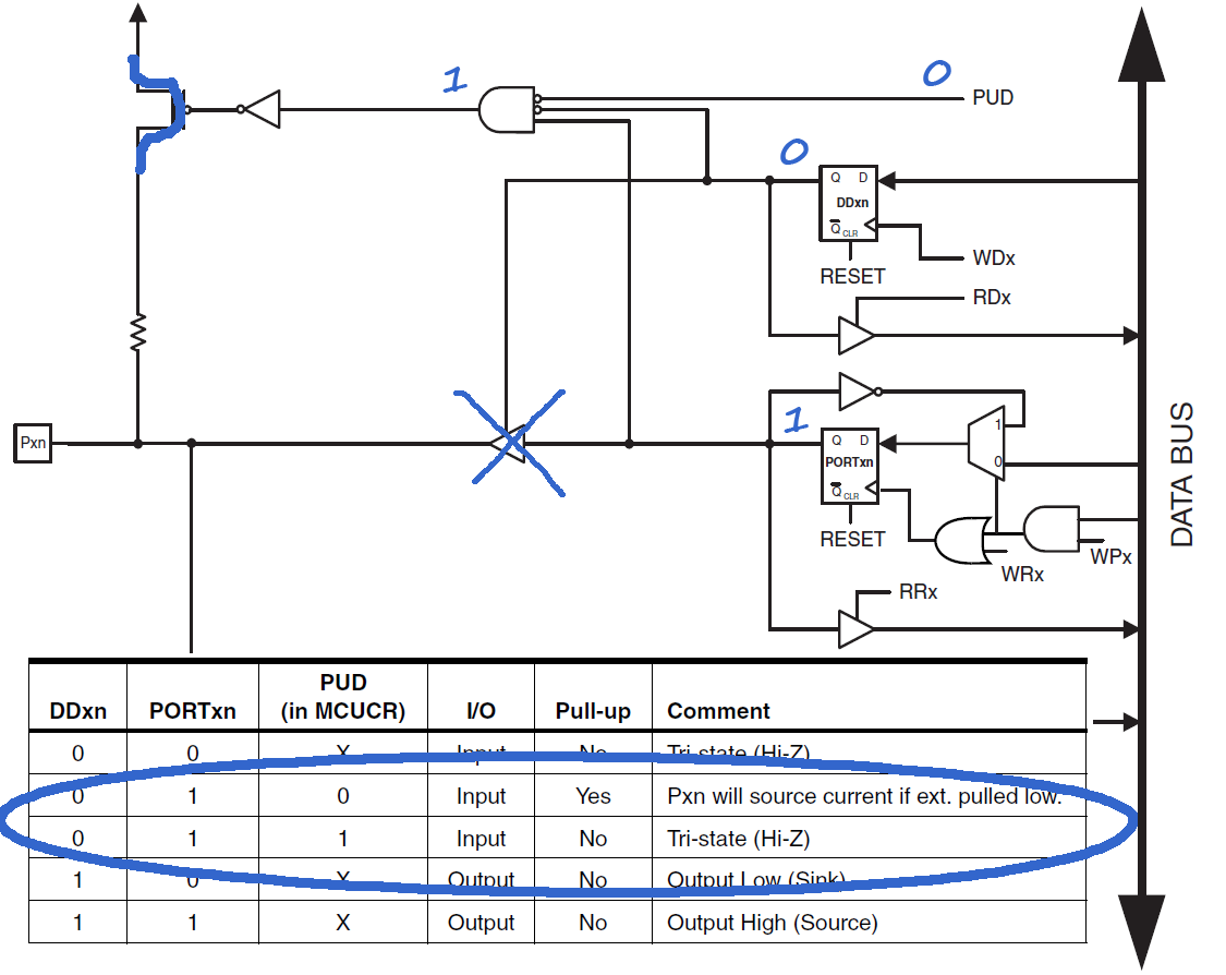
- To configure a Port (x) pin as an input set corresponding bit (n) in the Data Direction Register (DDxn) to 0. To add a pull-up resistor set the corresponding bit (n) of the PORTxn register to 1 (see illustration).
- You can now read the state of the input pin by reading the corresponding bit (n) of the PINxn
ACCESSING GPIO LINES IN ASSEMBLY and C++
DESIGN EXAMPLE 1 – Initialize 3DoT
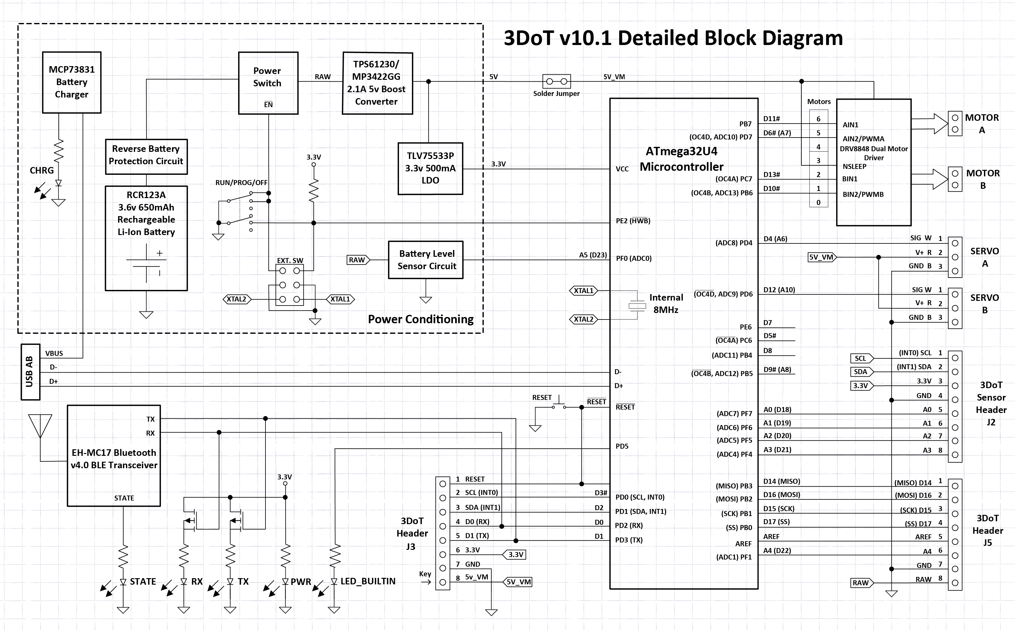
Problem: When power is applied to the ATmega32U4 on the 3DoT board, it needs to be configured. However, because the 3DoT board, like the Arduino UNO, is itself integrated into another system, it is not completely aware of its environment. Therefore, pins allocated to the shields should not be modified.
The following tables show how the code should configure Ports B (PB7..PB0), C (PC7,PC6), D (PD7..PD0), E (PE6,PE2), F (PF7..PF4,PF1,PF0).
Port B
| PIN | PB7 | PB6 | PB5 | PB4 | PB3 | PB2 | PB1 | PB0 |
| J5-1 | J5-2 | J5-3 | J5-4 | |||||
| NET | AIN1 | BIN2 | NC | NC | MISO | MOSI | SCK | SS |
| DDRB | 1 | 1 | 0 | 0 | X | X | X | X |
| PORTB | 0 | 0 | 1 | 1 | X | X | X | X |
/* undefind pins are not changed */
/* pins that are not connected are defined as inputs with pull-up resistors */
DDRB  &= 0x0F;   // clear most significant nibble
DDRB  |= 0xC0;   // set bit pattern
PORTB &= 0x0F;   // clear most significant nibble
PORTB |= 0x30;   // set bit pattern
Port C
| PIN | PC7 | PC6 | PC5 | PC4 | PC3 | PC2 | PC1 | PC0 |
| NET | BIN1 | NC | – | – | – | – | – | – |
| DDRC | 1 | 0 | – | – | – | – | – | – |
| PORTC | 0 | 1 | – | – | – | – | – | – |
DDRC  &= 03F;  // clear most significant 2 bits
DDRC  |= 0x80; // set bit pattern
PORTC &= 03F;  // clear most significant 2 bits
PORTC |= 0x40;
Port D
| PIN | PD7 | PD6 | PD5 | PD4 | PD3 | PD2 | PD1 | PD0 |
| Servo A | LED | Servo B | J1-5 | J1-4 | J3-3 | J3-2 | ||
| NET | AIN2 | SIG | BUILTIN | SIG | TX | RX | SDA | SCL |
| DDRD | 1 | 1 | 1 | 1 | X | X | X | X |
| PORTD | 0 | 0 | 0 | 0 | X | X | X | X |
DDRD  |= 0xF0; // set most significant nibble
PORTD &= 0x0F; // clear most significant nibble
Port E
| PIN | PE7 | PE6 | PE5 | PE4 | PE3 | PE2 | PE1 | PE0 |
| S-1 | ||||||||
| NET | – | NC | – | – | – | SW | – | – |
| DDRE | – | 0 | – | – | – | 0 | – | – |
| PORTE | – | 1 | – | – | – | 0 | – | – |
DDRE  &= 0xBB;  // clear bits 6 and 2
PORTE &= 0xBB;  // clear bits 6 and 2
PORTE |= 0x40;  // set bit pattern
Port F
| PIN | PF7 | PF6 | PF5 | PF4 | PF3 | PF2 | PF1 | PF0 |
| J2-5 | J2-6 | J2-7 | J2-8 | J2-6 | ||||
| NET | A0 | A1 | A2 | A3 | – | – | A4 | BATT |
| DDRF | X | X | X | X | – | – | X | 0 |
| PORTF | X | X | X | X | – | – | X | 0 |
DDRF &= 0xFE;
PORTF &= 0xFE;
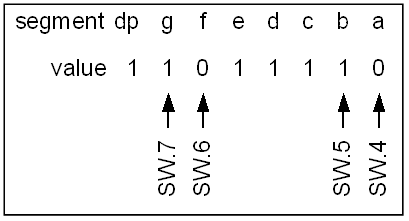
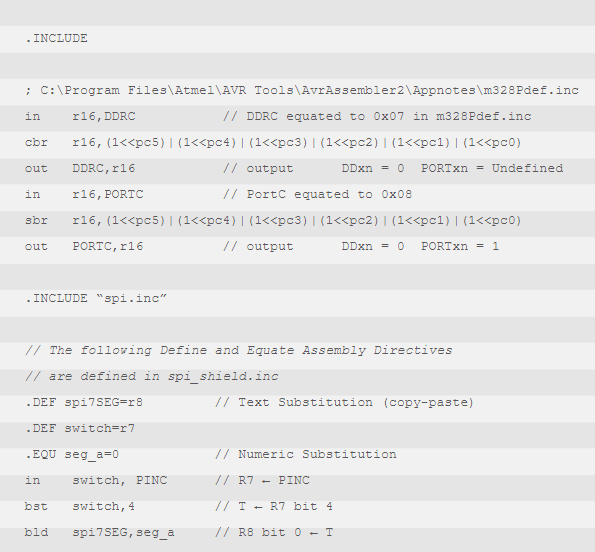
DESIGN EXAMPLE 2 – CSULB Shield Read Switches
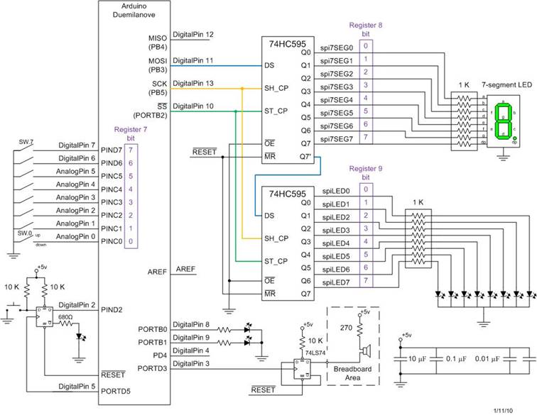
Problem: Program GPIO Port C bits 5 to 0 as inputs with pull-up resistors. For assembly version, read GPIO Port C into register r7 and move bit 4 to register r8 bit 0. Your programs should not modify Port C bits 7 and 6.
Arduino Script
// Analog pins0,1,2,3,4,5 map to Digital pins 14, 15, 16, 17, 18, 19
pinMode(14, INPUT_PULLUP);    // set pin to input with pullup resistor
Repeat this 1 line for pins 15, 16, 17, 18, and 19.
C++
DDRC &= ~0b00111111;
PORTC |= 0b00111111;
Assembly
; Initialize Switches with Pull-up resistors

in    r16, DDRC       // Port C DDR for switches 5 to 0
cbr   r16,0b00111111  // define bits 5 to 0 as input (clear)
out   DDRC,r16        // output      DDxn = 0  PORTxn = Undefined

in    r16,PORTC       // PORT C Register for switches 5 to 0
sbr   r16,0b00111111  // add pull-up resistors (PUR)
out   PORTC,r16       // output      DDxn = 0  PORTxn = 1

Main:
  :
in    r7,0x06         // R7 ← PINC
bst   r7,4            // T ← R7 bit 4
bld   r8,0            // R8 bit 0 (seg_a) ← T
.
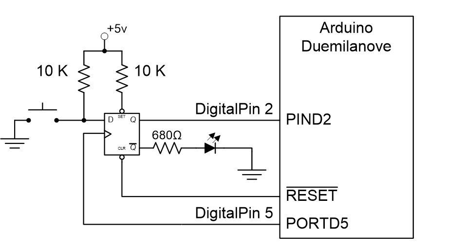
DESIGN EXAMPLE 3 – CSULB Shield Configure D Flip-Flop
Problem: Program GPIO Port D bit 5 as an output and bit 2 as an input without a pull-up resistor.
Arduino Script
// Variable definitions
const int dff_clk = 5;      // D flip-flop clock wired to digital pin 5
const int dff_Q = 2;        // D flip-flop Q output wired to digital pin 2
                            // Initialize digital pin 5 (dff_clk) as an
                            // output and digital pin 2 (dff_Q) as an input
pinMode(dff_clk, OUTPUT);   // set pin as output
digitalWrite(dff_clk, LOW); // initialize to zero
pinMode(dff_Q, INPUT);      // set pin as input
C++
// Preprocessor directives
#define dff_clk PORTD5
#define dff_Q PIND2

// Initialize push-button debounce circuit
DDRD |= 1 << dff_clk;     // define bit 5 of Data Direction Register
                          //(DDR)PORT D as an output
PORTD &= ~(1 << dff_clk); // initialize to zero
DDRD &= ~(1 << dff_Q);    // define bit 2 of Data Direction Register
                          //(DDR)PORT D as an input
PORTD &= ~(1 << dff_Q);   // without a pull-up resistor
Assembly
; Assembly directives
.EQU dff_clk=PORTD5
.EQU dff_Q=PIND2

; Initialize push-button debounce circuit
  sbi   DDRD, dff_clk   // flip-flop clock, DDRD5 = 1 PORTD5 = Undefined
  cbi   PORTD, dff_clk  //                  DDRD5 = 1 PORTD5 = 0
  cbi   DDRD, dff_Q     // flip-flop Q      DDRD2 = 0 PORTD2 = Undefined
  cbi   PORTD, dff_Q    //                  DDRD2 = 0 PORTD2 = 0
ATmega32U4 Register Summary and the I/O Port
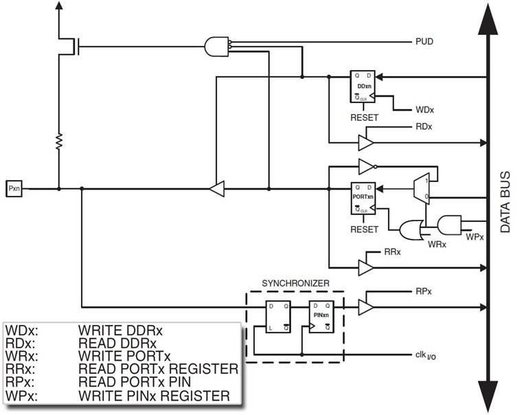
- Three I/O memory address locations are allocated for each port, one each for the Data Register – PORTx, Data Direction Register – DDRx, and the Port Input Pins – PINx.
- The Port Input Pins I/O location PINx is Read Only, while the Data Register and the Data Direction Register are read/write.
- However, Writing a logic one to a bit in the PINx Register, will result in a Toggle in the corresponding bit in the Data Register.
- In addition, the Pull-up Disable – PUD bit in MCUCR disables the pull-up function for all pins in all ports when set.
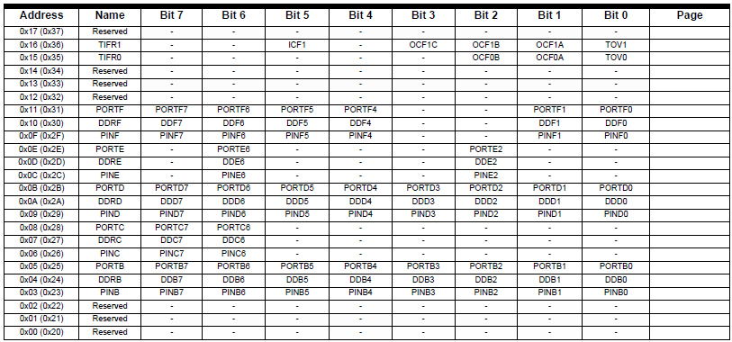
Figure 2. Register Summary
I/O PORT PIN SCHEMATIC
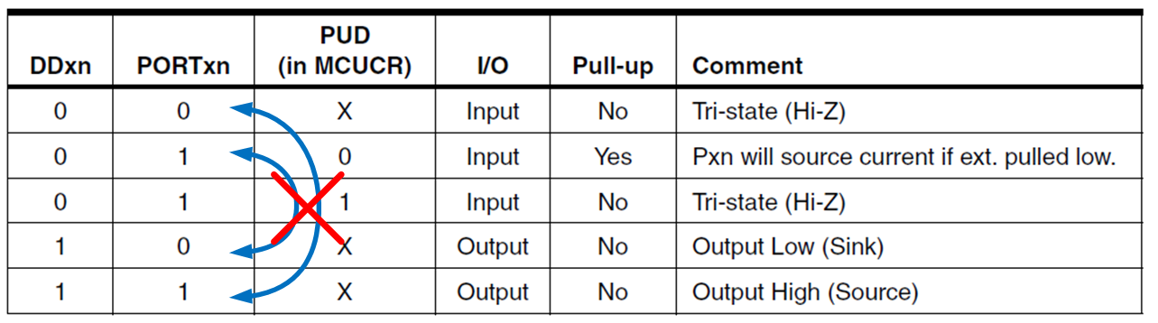
I/O PORT PIN CONFIGURATIONS
.
Appendix A – PROGRAM I/O PORT AS AN INPUT USING MNEMONICS
In the original Read Switches example, I programmed GPIO Port C bits 5 to 0 as inputs with pull-up resistors. Read GPIO Port C into register r7 and moved bit 4 to register r8 bit 0. In addition the program did not modify Port C bits 7 and 6. In this version, mnemonics and the shift operator are used to increase clarity (i.e., make the code more self documenting).
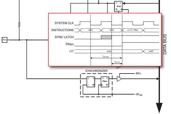
Appendix B – I/O PORT PIN “SYNCHRONIZER”
- As previously discussed, you read a port pin by reading the corresponding PINxn Register bit. The PINxn Register bit and the preceding latch constitute a synchronizer. This is needed to avoid metastability if the physical pin changes value near the edge of the internal clock, but it also introduces a delay as shown in the timing diagram.
- Consider the clock period starting shortly after the first falling edge of the system clock. The latch is closed when the clock is low, and goes transparent when the clock is high, as indicated by the shaded region of the “SYNC LATCH” signal. The signal value is latched when the system clock goes low. It is clocked into the PINxn Register at the succeeding positive clock edge. As indicated by the two arrows tpd,max and tpd,min, a single signal transition on the pin will be delayed between ½ and 1½ system clock period depending upon the time of assertion.
Appendix C – SWITCHING BETWEEN I/O PORT PIN CONFIGURATIONS
- When switching between tri-state ({DDxn, PORTxn} = 0b00) and output high ({DDxn, PORTxn} = 0b11), an intermediate state with either pull-up enabled ({DDxn, PORTxn} = 0b01) or output low ({DDxn, PORTxn} = 0b10) must occur.
- Switching between input with pull-up ({DDxn, PORTxn} = 0b01) and output low ({DDxn, PORTxn} = 0b10) generates the same problem. You must use either the tri-state ({DDxn, PORTxn} = 0b00) or the output high state ({DDxn, PORTxn} = 0b11) as an intermediate step.