Fall 2016 Prosthetic Hand: Evolution of PCB Layout
Design and Manufacturing Engineer – Wilson Mach
This was my first experience with Eagle CAD, a software that allows the user to generate a schematic and use that schematic to transfer the entire circuit to a circuit board, which then get printed by a manufacturer that produces Printed Circuit Boards (or PCBs). I had a couple of basic circuits layout trainings from my Division Manager, Thanh Truc Le, and our goal was to make our PCB as small as possible to fit the entire circuit into a forearm junction. My understanding was to do just that and to do a DRC (Design Rules Check) which checks the entire board to make sure there are no errors in overlapping wires, enough space for each routed wire, via, components, etc. If there were no errors, then the board was good for manufacturing.
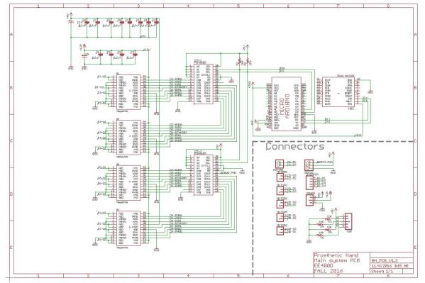
Figure 1 – PCB Schematic
Eagle CAD view of the schematic with all wiring and components labeled. All the component parts would be Surface Mount Devices (SMD) using Surface-Mount Technology (SMT).
Figure 2 – First Draft of Components and Design Placement with Division Approval
This was the first try without routing. This was a rough design on where each component should be placed. Only the blue circle was approved by the division manager.
Figure 3 – Version 2
This was the second try with a different design layout to fit the board with better routing. The yellow lines are called air wires which need to connect from component to component. I tried to have each component linked with a straight wire and avoid any crossings. No wires should cross or overlap, so each wire will have its own space on each layer (top or bottom).
Figure 4 – Routed wires with Different Design Layout to Fit on the Board
I routed most of the wires but was stuck on the leftover wires that were required for connection. Red colored wires indicate the top layer while blue colored wires indicate the bottom layer. Green circles are called vias and they link the top layer to the bottom layer. The green circles that are inside the component are male pinheads for female adapter connections.
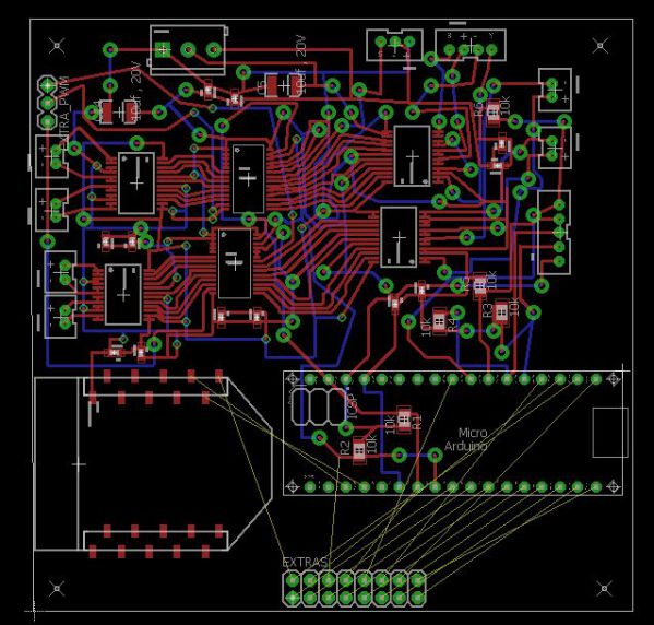
Figure 5 – Completed Routing and Added Extra Pins
In this version, all components were placed and routed. I did not realize that we could place the Xbee board and Arduino Micro on top and bottom layers. This realization helped me save much more space, because the Micro and Xbee connects into socket pins that have quarter inch stand bridges that goes on top of the IC. This version has all the components on the top layer only.
Figure 6 – Second PCB Schematic with More Capacitors
More capacitors were added for coupling purpose. These were added for each motor driver IC, I2C, Arduino Micro, and Xbee.
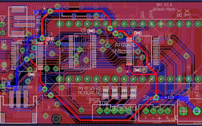
Figure 7 – Completed Routing with Power Line and Fixed 45 degree angles on Each Wire
This version is much improved compared to the last one. Using both layers to place some of the ICs on the bottom layer saved lots of space. The design placed 2 small capacitors next to each power output of the motor driver ICs and one for all the other ICs. The board was shrunk to 1.35×2.60 inches. Thicker power wires were used for the 5V and 12V to allow current to flow without heat. This board made the clearance on all spacing requirement that were specified by the manufacturer.
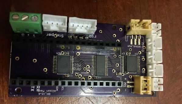
Figure 8 – Final Manufactured Version
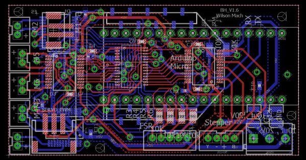
This is another improved version with a power plane for both 12V and 5V to make sure all the power can be distributed as close to the ICs as possible without any loss of current. Then, the rest of the plane will be copper filled and grounded. I replaced servo and motor adapters to be on the top layer. I labeled all components and wires to have an easier reference when placing the SMD on the board for soldering. Finally, I labeled all text in white color and white circles on the corners as drill holes for screw to lock down the PCB, if necessary.
Figure 9 – PCB Bottom View
There are two large capacitors near the power output for stability. All components made as SMD through SMT using an oven, placing each side at a time. The quarter inch socket stand is on this layer for the Xbee to be connected, leaving spaces on the bottom of the bridge to maximize space usage.
Figure 10 – PCB Top View without Micro
This is the completed PCB (without Arudino Micro) showing all the adapters for the 7 actuators and 4 force sensitive resistors (FSRs), as well as 1 servo driver. The green captive screw, or Phoenix connector, in the adapter on the bottom right corner is for the power output.
The entire process took a couple of weeks from the beginning to the final version of the PCB layout. Thanks to many members that helped me throughout the process to improve upon each version, as there were many errors and mistakes on the first version. The final version was approved by several manufacturers prior to getting it printed. I had a great experience and practice on this PCB layout.
