Serial Communications and SPI
Table of Contents
Reference(s):
The AVR Microcontroller and Embedded Systems using Assembly and C) by Muhammad Ali Mazidi, Sarmad Naimi, and Sepehr Naimi
- Chapter 5: Arithmetic, Logic Instructions, and Programs
- Section 5.4: Rotate and Shift Instructions and Data Serialization
- Chapter 7: AVR Programming in C
- Section 7.5 Data Serialization in C
- Chapter 11: AVR Serial Port Programming in Assembly and C
- Section 11.1 Basics of Serial Communications only (You are not responsible for Sections 11.2 to 11.5)
- Chapter 17: SPI Protocol and MAX7221 Display Interfacing
- Section 17.1 SPI Bus Protocol
Additional Resource Material
- Fairchild Semiconductor MM74HC595 “8-Bit Shift Register with Output Latches” document MM74HC595.pdf
- Arduino Wire Library http://www.arduino.cc/en/Reference/Wire
- Arduino Interfacing with Hardware http://www.arduino.cc/playground/Main/InterfacingWithHardware
Location of Arduino Wire Library C: \Program Files (x86)\ arduino-0017\ hardware\ libraries
Location of #include files stdlib.h, string.h, inttypes.h C: \Program Files (x86)\arduino-0017\ hardware\tools\avr\avr\include
Location of #include file twi.h (1 of 3) C: \Program Files (x86)\arduino-0017\ hardware\tools\avr\avr\include\compat
Introduction
Taking the bits apart and putting them back together again.

Figure 1. Lieutenant Reicher at Farpoint Station, Planet Deneb IV
ATmega32U4 SPI Features
- Full-duplex, Three-wire Synchronous Data Transfer
- Master or Slave Operation
- LSB First or MSB First Data Transfer
- Seven Programmable Bit Rates
- End of Transmission Interrupt Flag
- Write Collision Flag Protection
- Wake-up from Idle Mode
- Double Speed (CK/2) Master SPI Mode.
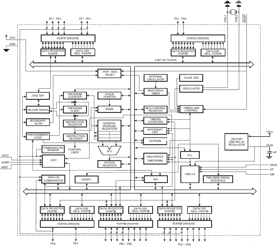
Figure 2. ATmega32U4 Block Diagram
What is a Flip-Flop and a Shift Register
You can think of a D flip-flop as a one-bit memory. The something to remember on the D input of flip-flop is remembered on the positive edge of the clock input.
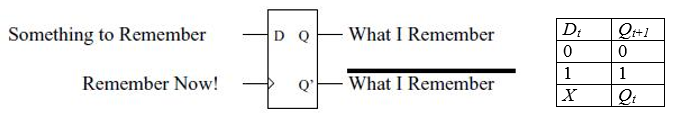
Figure 3. D Flip-Flop Truth Table
A data string is presented at ‘Data In’, and is shifted right one stage on each positive ‘Clock’ transition. At each shift, the bit on the far left (i.e. ‘Data In’) is shifted into the first flip-flop’s output (i.e., ‘Q’). Source: http://en.wikipedia.org/wiki/File:4-Bit_SIPO_Shift_Register.png
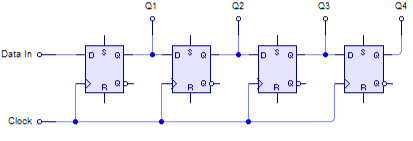
Figure 4. Basic Shift Register
What is a Serial Shift Register with Parallel Load
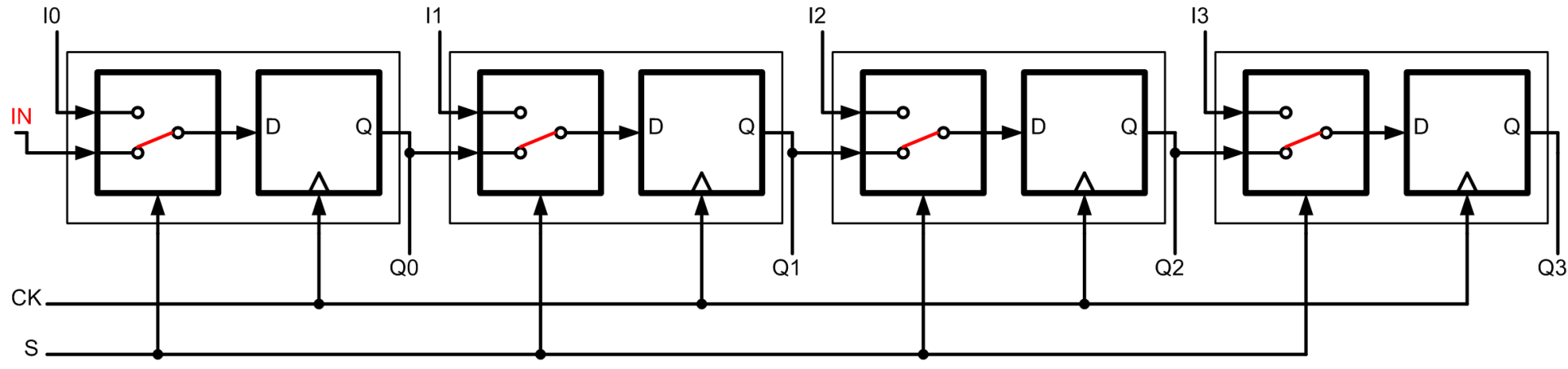
Figure 5. Functional drawing of a parallel-in/serial-out shift register
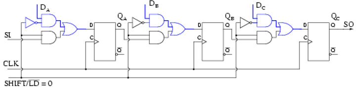
Figure 6. Parallel-in/serial out shift register using logic gates
Setup and Hold Times
- For a positive edge triggered Flip-flop, the setup time is the minimum amount of time before a rising clock edge occurs that a signal must arrive at the input of a flip-flop in order for the flip-flop to read the data correctly.
- Likewise, the hold time is the minimum time a signal must remain stable after the rising clock edge occurs before it can be allowed to change.
- The propagation delay is the maximum amount of time after the positive clock edge to when you can expect to see the signal on the output.
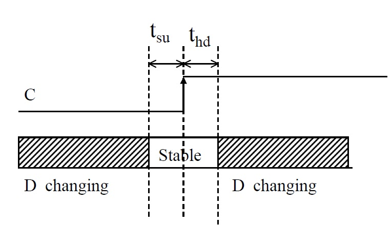
Figure 7. Setup and Hold Times
Ten Questions that need answers before you can design a Serial Peripheral Interface
Configuration and Control
- Master/Slave Select Who is the Master and who is the Slave? Specifically, which subsystem contains the clock?
- SPI Clock Rate Select At what clock frequency (divisor) is the data transmitted/received by the Master?
- Data Order In what order is the data transmitted (msb or lsb first)?
- Clock Polarity & Phase How is the data transmitted relative to the clock (data setup and data sampled)
- SPI Slave Select How do you address a slave(s) device?
- SPI Interrupt Enable Will you use polling or interrupts to monitor data transfer operations?
Send/Receive Data
- SPDR Write How do you write data to the SPI Data Register?
- SPDR Read How do you read data to the SPI Data Register?
Monitoring and Status Questions
- SPI Interrupt Flag How do you know when a data transfer operation is done?
- Write Collision Flag How do you detect if a byte of data was written to the shift register during a data transfer operation (read or write).
SPI Overview – Serial Communication
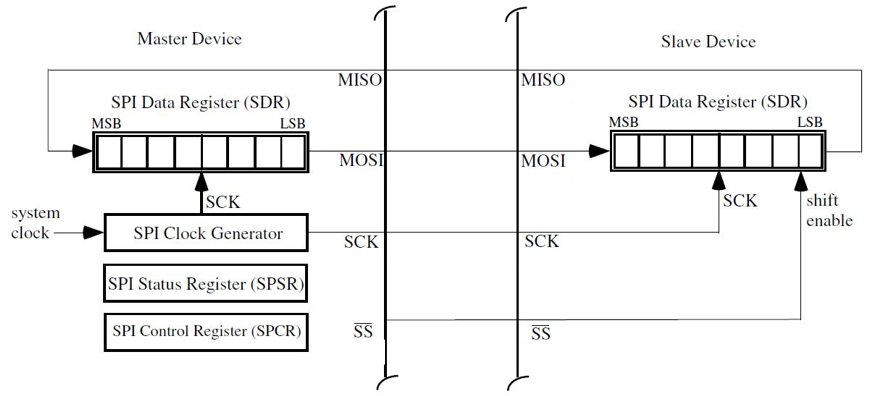
Figure 8. SPI Block Diagram with Registers
SPI Overview – The Registers
- SPI Control Register – You configure the SPI subsystem by writing to the SPI Control Register (SPCR) and the SPI2X bit of register SPSR. The ATmega328P SPI subsystem may be configured as a master a slave or both. Setting bit SPE bit enables the SPI subsystem.
- SPI Data Register – Once enabled (SPE = 1), writing to the SPI Data Register (SPDR) begins SPI transfer.
- SPI Status Register – The SPSR register contains the SPIF flag. The flag is set when 8 data bits have been transferred from the master to the slave. The WCOL flag is set if the SPI Data Register (SPDR) is written during the data transfer process.
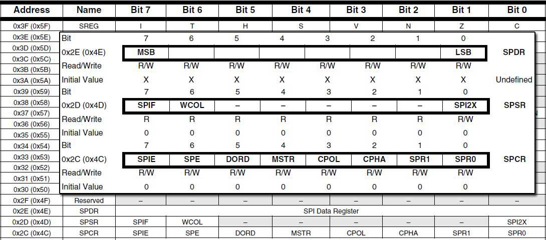
Figure 9. SPI Registers
How to Configure the SPI Subsystem
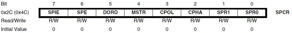
Figure 10. SPCR
SPI Interrupt Enable
This bit causes the SPI interrupt to be executed if the SPIF bit in the SPSR Register is set and if the Global Interrupt Enable bit in SREG is set. For our design example we will be polling the SPIF bit. Consequently, we will leave the SPIE bit in its default (SPIE = 0) state.
SPI Enable
When the SPE bit is one, the SPI is enabled. This bit must be set to enable any SPI operations.
Data Order
When the DORD bit is one (DORD = 1), the LSB of the data word is transmitted first, otherwise the MSB of the data word is transmitted first. For the Arduino Proto-shield, we want to transfer the most significant bit (MSB) bit first. Consequently, we will leave the DORD bit in its default (DORD = 0) state.
MSTR: Master/Slave Select
This bit selects Master SPI mode when set to one, and Slave SPI mode when cleared. For our design example, the ATmega32U4 is the master and the74HC595 “8-bit Shift Register with Output Latches” is the slave. Consequently, we need to set the DORD bit to logic 1 (MSTR = 1). Note: I am only telling you part of the story. If you want to configure the ATmega328 to operate as a slave or master/slave please see the datasheet.
Clock Polarity and Clock Phase
The Clock Polarity (CPOL) and Clock Phase (CPHA) bits define how serial data is transferred between the master and the slave. These SPI Data Transfer Formats are defined in Figure 10.
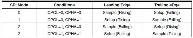
Figure 11. SPI Modes of Operation
SPI Clock Rate Select Bits SPI2X , SPR1, SPR0
These three bits control the SCK rate of the Master. In our design example, the ATmega32U4 is the Master. These bits have no effect on the Slave. The relationship between SCK and the Oscillator Clock frequency fosc is shown in the following table. For our design example we will be dividing the system clock by 16.
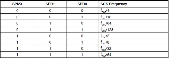
Figure 12. SPI Prescaler
SPI Code Example
For our example we are going to use the ATmega32U4 SPI subsystem to send a byte of data to a 74HC595 “8-Bit Shift Register with Output Latches” The interconnection between Master and Slave consists of two shift Registers, and a Master clock generator. For our example the ATmega’s SPI subsystem is the Master and the 74HC595 “8-Bit Shift Register with Output Latches” is the slave.
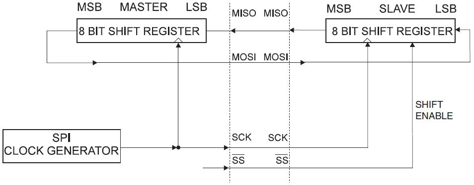
Figure 13. SPI Block Diagram
Overview of the 74HC595
- The 74HC595 “8-bit Shift Register with Output Latches” contains an eight-bit serial-in (SER), parallel-out (QH to QA), shift register that feeds an eight-bit D-type storage register.
- The storage register has eight 3-state outputs, controlled by input line G.
- Separate positive-edge triggered clocks are provided for both the shift register (SCK) and the storage register (RCK)
- The shift register has a direct overriding clear (SCLR), serial input, and serial output (standard) pins for cascading (Q’H).
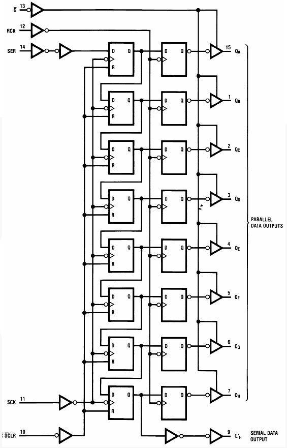
Figure 14. 74HC595 Block Diagram
For our design example, we want data to be clocked into the 74HC595 on the Rising clock edge (the D-flip-flops of the 74HC595 are positive edge triggered), as shown in the Figure below. Consequently, we want the ATmega32U4 to Setup the data on the serial data out line (SER) on the Trailing clock edge. Looking at Table 18-2 we see that this corresponds to SPI Mode = 0.
Figure 15. SPI Serial Write Timing Diagram
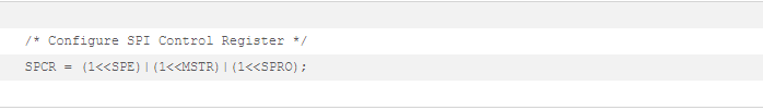
Configure SPCR
In this example, the SPI peripheral subsystem will be configured to send 8-bits of data a 74HC595. Reviewing the last three pages, to configure the SPI subsystem for the CSULB Shield.
Figure 16. SPCR
- We will be polling the SPI Interrupt flag (SPIE = 0)
- Enable the SPI Subsystem (SPE = 1)
- Set Data Order to transmit the MSB first (DORD = 0)
- Define ATmega32U4 as the Master (MSTR = 1)
- Configure the SPI to clock data (sample) on the rising edge and change data (setup) on the falling edge. (CPOL = 0, CPHA = 0)
- Set prescalar to divide system clock by 16 (SPR1 = 0, SPR0 = 1)
tl;dr SPCR = 0x51
C Code Example
Assembly Code Example
ldi r16, 0x51
out SPCR, r16
Test Your Knowledge
- The above code assumes that the SPI2X bit in the SPI status register (SPSR) can be left at its default value (SPI2X = 0). How would you explicitly clear this bit in C++ and/or Assembly?
- The above code does not include the instructions to initialize the Data Direction registers for DD_MOSI (Port B bit 3), the SPI clock DD_SCK (Port B bit 5), or our SS signal PB2 (Port B bit 2). How would you write the code in C++ and/or Assembly to initialize the SPI data direction register DDR_SPI (Port B DDR) so these pins were outputs?
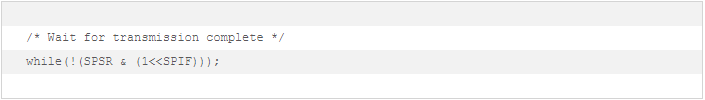
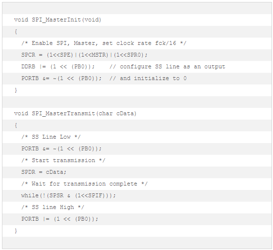
How to Operate the SPI Subsystem – Polling –
- Writing a byte to the SPI Data Register (SPDR) starts the SPI clock generator, and the hardware shifts the eight bits into the Slave (74HC595). The Master generates the required clock pulses on the SCK line to interchange data.
C Code Example
/* Start Transmission */
SPDR = data;            // data is an 8-bit variable in SRAM
Assembly Code Example
out SPDR,data // data is in register r8
- Data is always shifted from Master-to-Slave on the Master Out Slave In (MOSI) line, and from Slave-to-Master on the Master In Slave Out (MISO) line.
- After shifting one byte, the SPI clock generator stops, setting the end of Transmission Flag (SPIF bit in the SPSR register). If the SPI Interrupt Enable bit (SPIE) in the SPCR Register is set, an interrupt is requested. The Master may continue to shift the next byte by writing it into SPDR. In our lab we used polling to monitor the status of the SPIF flag.
C Code Example
Assembly Code Example
wait: in    r16,SPSR
      bst   r16,SPIF
      brtc  wait
      ret
- After the last data packet is transmitted, the Master will transfer the data to the eight-bit D-type storage register of the slave by strobing the slave select (SS) line. When configured as a Master, the SPI interface has no automatic control of the SS line. This must be handled by your software. Note: We are using the SS line in a non-standard fashion. If you want to configure the ATmega32U4 to operate as a master, slave, or master/slave using the Atmel convention, please see the datasheet.
C Code Example
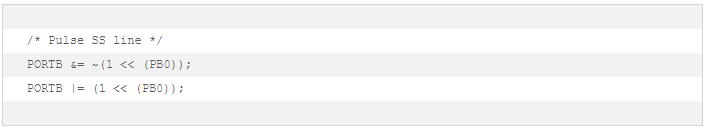
Assembly Code Example
cbi  PORTB,PB0
sbi  PORTB,PB0
SPI C++ Code Example
SPI Assembly Code Example
; SPI interface registers
.DEF data=r8

InitShield:
  ldi   r16, 0x51
  out   SPCR, r16
ret

WriteDisplay:
  ; Start transmission of data
  cbi   PORTB,PB0   // ss line active low
  out   SPDR,data
  rcall SpiTxWait
  sbi   PORTB,PB0   // ss line high
  ret

SpiTxWait:
  ; Wait for transmission complete
  push r16
wait:
  in   r16,SPSR
  bst  r16,SPIF
  brtc wait
  pop r16
  ret
Appendix A Detail Description of the 74HC595
Tri-State Output Buffers
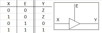
Figure 17. Tri-State Buffer
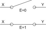
Figure 18. Tri-state Buffer Functional Diagram
74HC595 Storage Registers (D-Flip Flops)
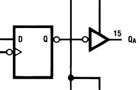
Figure 19. 74HC595 Storage Register
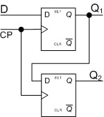
Figure 20. 74HC595 Serial Shift Register Wiring
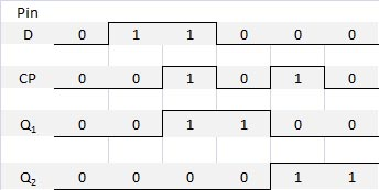
Figure 21. 74HC595 Shift Operation Example
Review Questions
- TBD
Answers
Using your mouse, highlight below in order to reveal the answers.
- TBD