Spring 2016 A-TeChToP Seizure Watch PCB Layout
By Marena William (Manufacturing Engineer)
Overview
The 3D printed housing of the seizure watch will contain the PCB board which consists of the EDA sensor, accelometer, clock and the ATSAMB11. The electrodes’ wires will be connected to the EDA connector. Eagle CAD software was used to generate the PCB schematic and layout.
Table of Contents
Schematic
The schematic was created by Rose Leidenfrost (Electronics Engineer).
Prior to designing the PCB layout, some notes by the Electronics Division were taken into consideration.
- DGND and AGND are separate ground planes, side by side on the same layer, separated by as large a distance as possible, star connected using the three pad solder jumper.
- DGND is digital ground, associated with SAMB11, and ADXL345
- AGND is an analog ground associated with the EDA sensor, and the op amps (LM358).
- Capacitors: should be tantalum, despite their propensity for failure. Make the voltage rating greater than 5 times what it should be.
- C1 should be very close to the battery
- C3 and C5 should be very close to the op amp.
- C7 should be very close to ADXL345
- C9 should be very close to the SAMB11
- C10 should be very close to the EDA sensor.
- Battery. Consult manufacturing/systems to verify the correct battery package
- Debug/Programming connector. Consult manufacturing/systems.
- Crystal: Again, package type must be verified.
- SAMB11 Paddle connection: The bottom plate of the SAMB11 needs to be soldered to the ground plane with 9 vias (3X3) according to the datasheet. The footprint has holes and pads in the correct locations. Consult with team.
- The jumper called JP1 should be fairly close to the big 24 pin connector.
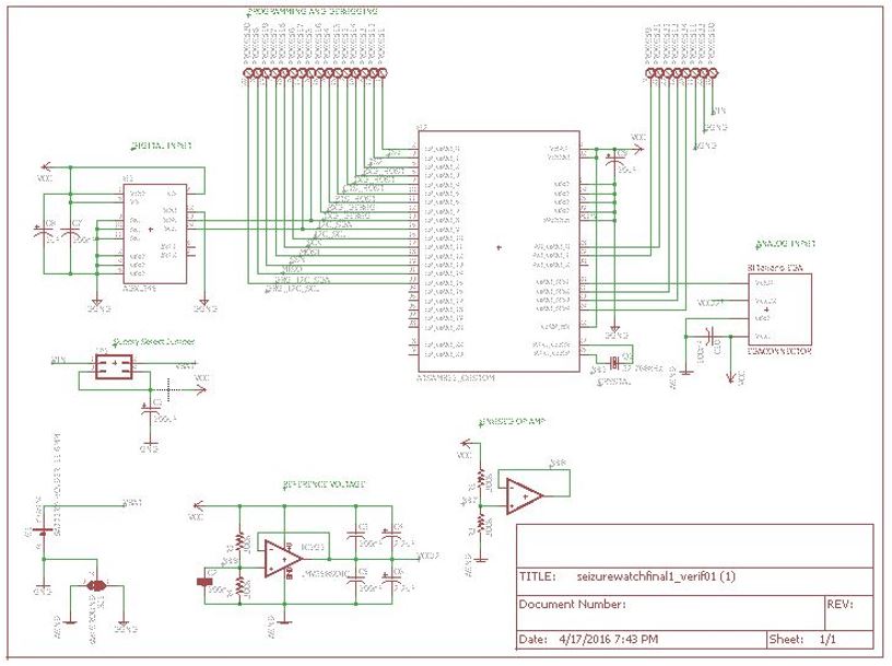
Figure 1: A-TechTop Seizure Watch Schematic by Rose Leidenfrost
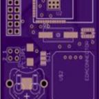
Layout
The PCB layout features two ground planes (AGND&DGND). The two planes are connected through the three pad solder jumper (SJ1). The 2 layer board has dimensions of 1.50×2.33 inches (38.10×59.06 mm).

Figure 2: A-TechTop Seizure Watch PCB Layout with dimensions in Eagle CAD
Manufacturing
The PCB will be manufactured by OSH Park (recommended by manufacturing division manager). Once the PCB is received, the components will be soldered by the manufacturing engineer.
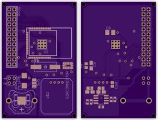
Figure 3: A-TechTop Seizure Watch PCB board based on manufacturer’s website. (left: top layer- right: bottom layer)