Eagle CAD Training
Written By: Muhannad Al Mohamed (E&C DM)
Table of Contents
Objective
This blog is intended to introduce Eagle CAD designing application to members to be able to design schematics for electronic circuits. The members of the E&C division are required to know how to make schematics of customed printed circuit boards (PCB) for their corresponding projects. These schematics can be used to design the layout version of the PCB in the Eagle CAD layout part. The layout of the PCB can then be used to generate Gerber files; which can be sent to fabrication houses to make the PCBs.
Creating New Sketch
To start a new sketch a new project should be created and a name should be given to it. After that, a new schematic should be created within the project.

Creating a new schematic
Adding Parts
To add a part from the EagleCAD library, the add icon should be clicked where the list of all the parts would show in a window.
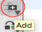
Add Icon
Parts can be chosen directly from the libraries by double-clicking on each part. The search window can be used to easily find a specific part. However, the EagleCAD search engine is literal; which means that any misspelling in the part name will not show any result. To avoid that, stars should be typed before and after the part’s name.
Placing parts
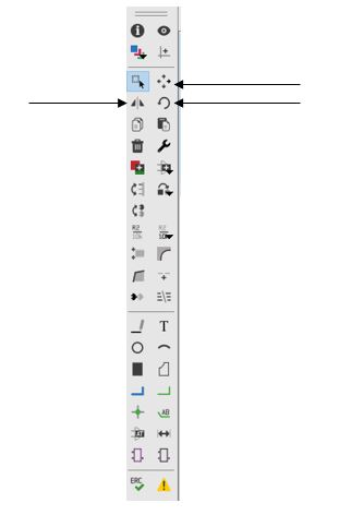
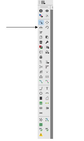
Placing a part is simple, one click should input parts into the schematic and by clicking escape twice it would quit the adding mode. To rotate parts, right click before placing any part. Rotation of a part or a group of parts can be obtained by clicking the rotate icons.
Rotating parts
Connecting Pins
To connect placed parts the net icon should be clicked. The edge of each pin should be clicked when connecting parts to ensure that you are connecting to the part not just drawing a line on it.

Net Icon
When connecting to a part make sure that a connecting window shows up asking for permission to connect to a part. When a connecting is done, double-clicking the crouser will quit the connecting mode.
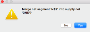
Connecting Window
When connecting a line with a line, make sure that a junction shows at the intersection. If there is no junction showing, a junction can be added by clicking the junction icon.

Junction Icon

Unconnected lines
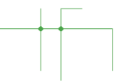
Connected lines
Labeling Pins and Parts
Parts can be given labels that can show names and values in both the schematic and PCB layout designs. To add a name label click on the name label and click on the desired part. A value label can be added to parts as well by clicking on the value label. Just a reminder, the value label is still just a name and does not have any relation to the part’s characteristics.

Name Icon
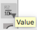
Value Icon
Pins can be named as well by giving them labels by clicking on the label icon and clicking on the desired pin.If a pin is named exactly with the same name to another pin, a window should pop up asking to connect the pins. If clicked true, the pins would be automatically connected without showing a line. The labels appearance can be changed by clicking on the tag icon and the size of the label can be changed as well.

Label Icon

Regular and Tag Icons
Changing Size Icon
EagleCAD Libraries
EagleCAD has a lot of different libraries from various retailers and manufacturers. It also has the regular parts such as supplies, passive components, .. etc. However, sometimes the desired part is not found in the EagleCAD built-in library so in that case a new library should be added.
Adding Libraries
To add a library, its “.lbr” file should be downloaded first from the manufacturers’ website or from different websites that provide eagle libraries:
Once the “.lbr” file is downloaded it should be placed in the “lbr” folder in the application’s folders. After that, the library should be indicated as used in the library manager window.
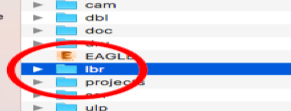
Placing library in lbr Folder
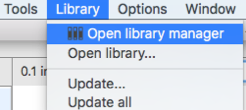
Library Manager
Using a Library
Testing
Verify Connected Pins
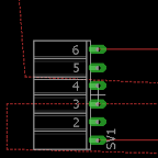
If the pins were labeled with similar names, their connection can be checked by clicking the show icon. Once the show icon is clicked, by clicking on any pin it would show the connected pins the clicked pin in bold font. It is very helpful to trace pins and check if all the parts are connected correctly.

Show Icon

Connected Pins
Checking Errors
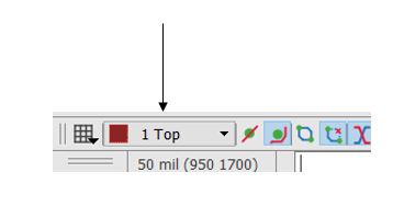
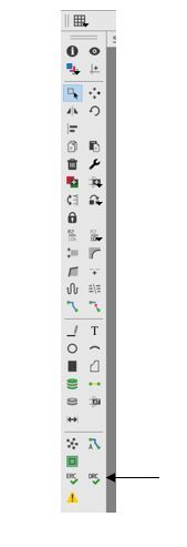
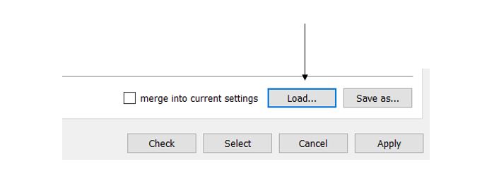
After creating the schematic, the design should be checked if it has any errors. By clicking on the ERC icon a window should pop up showing any electrical errors. Make sure that you have no errors befor going to the PCD layout part of designing.
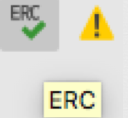
ERC Icon
Training Material
Schematic Training
Further trainings on creating EagleCAD schematics can be found here:
PCB Layout Training
Training on the making of the layout version of the custom PCB can be found in this blog written by Charles Banuelos (MFG DM).