By: Christine Vu (Missions, Systems, and Test)
Purpose
Verification Tests will be conducted to verify the requirements based on the Verification Matrix.
Requirements for Verification Tests
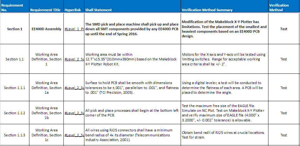
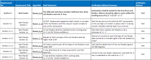
Section 1 EE400D Assembly
The SMD pick and place machine shall pick up and place down all SMT components provided by any EE400D PCB up until the end of Spring 2016.
Section 1.1
Working area must be within 12.2”x15.35”(310mmx390mm) based on the Makeblock X-Y
Plotter Robot Kit.
Section 1.1.2
Surface to hold PCB shall be smooth with dimensions tolerances to be ±.001″, parallelism to .001″, and flatness to .001″ (TCI Precision, 2005).
Section 1.1.3
All pick and place processes shall begin at the bottom left corner of the PCB.
Section 1.1.4
All wires using RJ25 connectors shall have a minimum bend radius of 4x its diameter (Telecommunications Industry Association, 2001).
Section 1.2
Pick and place SMD machine shall change the orientation of each SMT component before placement.
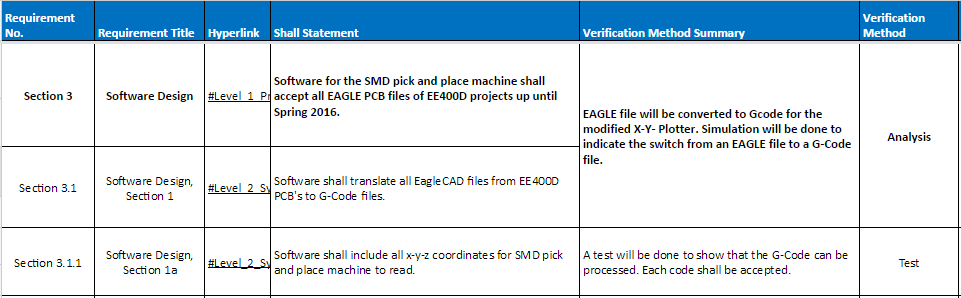
Section 3 Software Design
Software for the SMD pick and place shall accept all EAGLE PCB files of EE400D projects up until Spring 2016.
Section 3.1
Software shall translate all EagleCAD files from EE400D PCB’s to G-Code files.
Section 3.1.1
Software shall include all x-, y-, and z-coordinates for SMD pick and place machine to read.
Section 4 Reel Feeder Design
The SMD pick and place machine shall have four 8mm reel feeders and one IC tray.
Section 4.1
All SMT resistors and capacitors shall remain in cut-tape of the reel feeders until the vacuum nozzle is ready to pick up the component.
Section 4.1.1
All reel feeders shall be installed on the working area, 12.2”x15.35”(310mmx390mm).
Section 4.1.2
Bracket to hold cut-tape of the reel feeders shall be higher than 0.04″.
Section 4.1.3
All motors used to peel off cut-tape of reel feeders must rotate 360°.
Section 4.2
IC tray shall store all IC chips required for one PCB assembly.
Section 4.2.1
IC tray shall be installed within working area, 12.2”x15.35” (310mmx390mm).
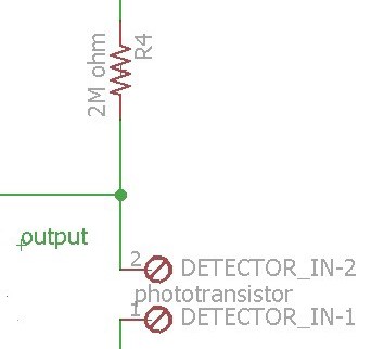
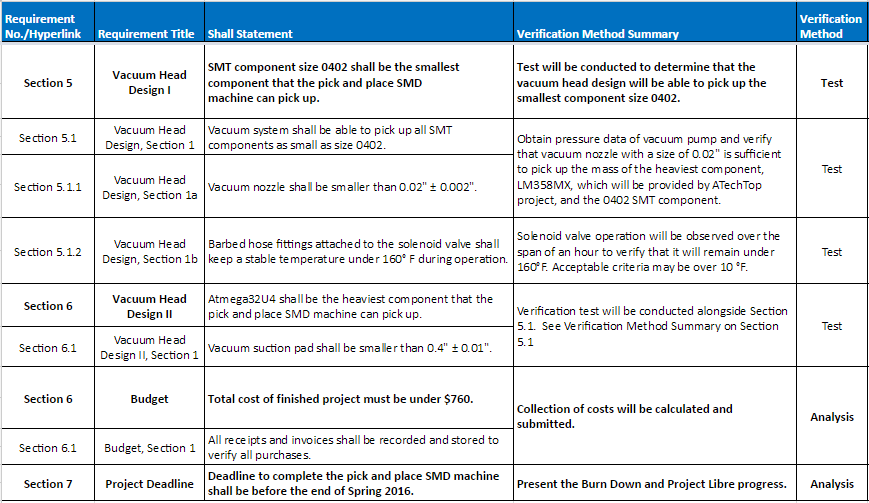
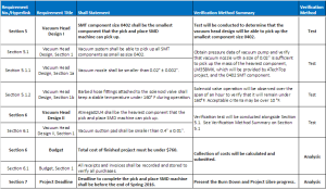
Section 5 Vacuum Head Design I
SMT component size 0402 shall be the smallest component that the pick and place SMD
machine can pick up.
Section 5.1
Vacuum system shall be able to pick up all SMT components as small as size 0402.
Section 5.1.1
Vacuum nozzle shall be smaller than 0.02″ ± 0.002″.
Section 6 Vacuum Head Design II
ATmega32u4 chip shall be the heaviest component that the pick and place SMD machine can pick up.
Section 6.1
Vacuum suction pad shall be smaller than 0.4″ ± 0.01″.
Summary of Verification
Verification tests will be conducted to reflect the requirements on the physical design of the SMD pick and place machine. A list of procedures will be presented in this document followed by the results and conclusion.
Verification Matrix

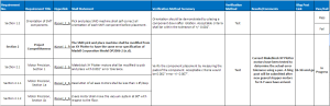
** Updated 4/29/16: Added new requirement section to consider the heaviest chip can be picked up. Dimension limitations were based on Atmel’s datasheet (2016).
List of Equipment
Applicable tools and software will be listed for each Verification test.
Verification Tests
EE400D Assembly
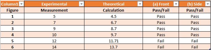
Working Area Test
Working area is defined by the area that includes PCB to assemble, reel feeders, and IC tray. To verify that our design meets the size criteria for working area, a test will be conducted to calculate its parameters.
Requirements
Section 1 EE400D Assembly
The SMD pick and place machine shall pick up and place down all SMT components provided by any EE400D PCB up until the end of Spring 2016.
Section 1.1
Working area must be within 12.2”x15.35”(310mmx390mm) based on the Makeblock X-Y
Plotter Robot Kit.
Section 1.1.2
Surface to hold PCB shall be smooth with dimensions tolerances to be ±.001″, parallelism to .001″, and flatness to .001″ (TCI Precision, 2005).
Section 1.1.3
All pick and place processes shall begin at the bottom left corner of the PCB.
Section 1.1.4
All wires using RJ25 connectors shall have a minimum bend radius of 4x its diameter (Telecommunications Industry Association, 2001).
Section 1.2
Pick and place SMD machine shall change the orientation of each SMT component before placement.
Applicable Tools
| Equipment Type |
Name (Brand) |
Tolerance |
| Mitutoyo S/N 12519090 |
Caliper |
0.001” |
| Measuring Tape |
Stanley 33-425 Powerlock 25-Foot by 1-Inch Measuring Tape |
+/- 3% |
Procedure
- Record the weight of the heaviest component.
- Calculate the required minimum diameter of the vacuum nozzle that the heaviest can be picked up.
- Test and measure the pressure.
- Attach the Z-Axis with pen attachment to the X-Y Plotter.
- Create an EAGLE PCB design by placing capacitors on each corner of the design. A free EAGLE version would allow 4” x 3.2”.
- Convert to GCode and send to Makeblock X-Y Plotter.
- After the sketch, measure the dimensions of the EAGLE PCB design.
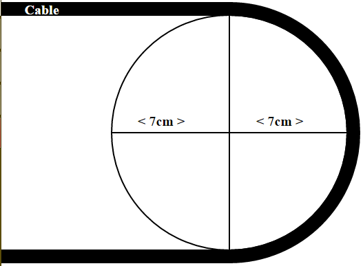
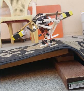
Cable Test
A test will be conducted to determine that the bending radius will not exceed a bend radius of 4x its radius.
Applicable Tools
| Equipment Type |
Name (Brand) |
Tolerance |
| Mitutoyo S/N 12519090 |
Caliper |
0.001” |
Procedure
- Connect the wires attached to the X-Axis and Y-Axis.
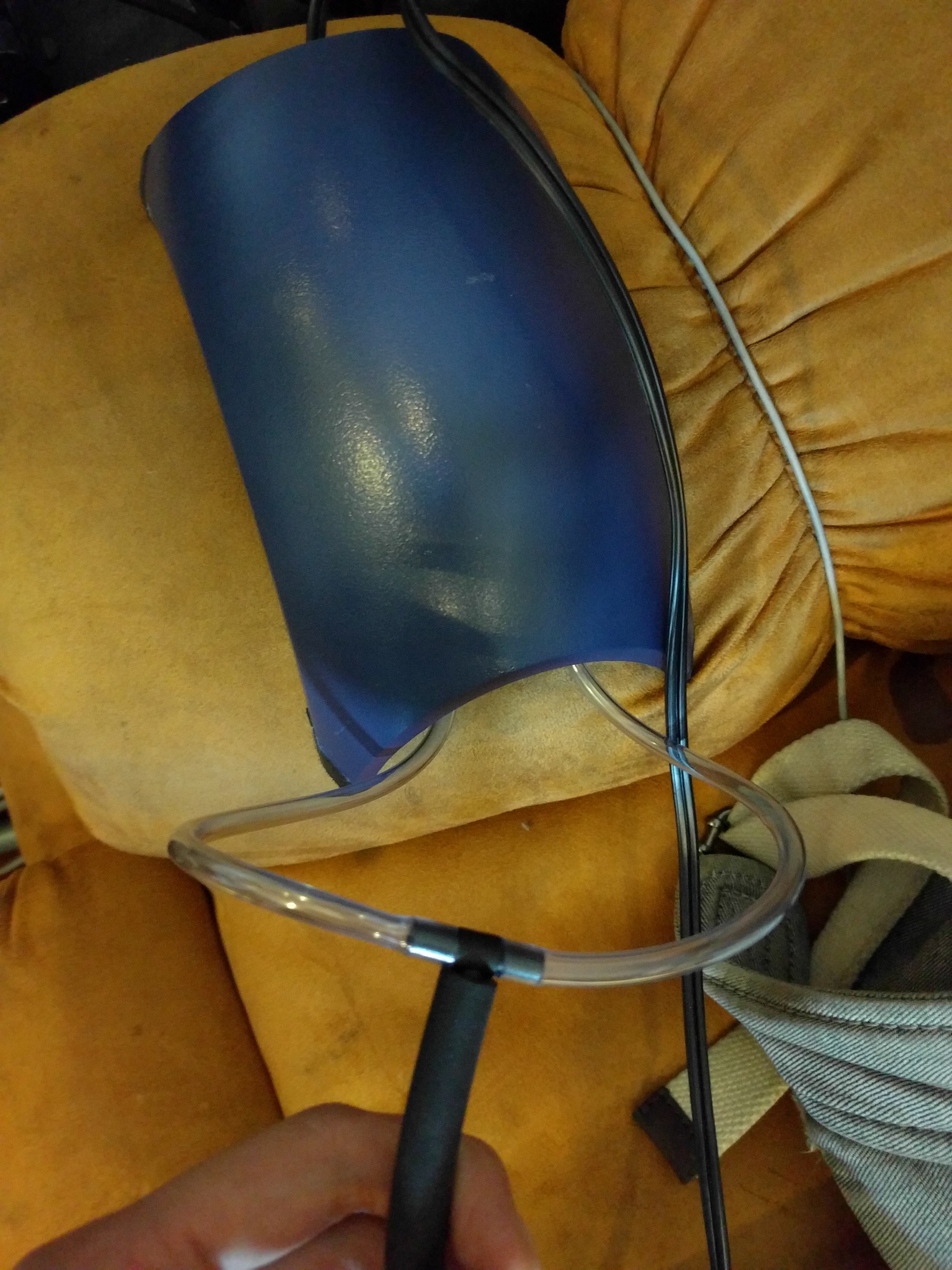
- Control the Y-Axis and move to the farthest end of the plotter with respect to the PCB until the limiting switch is hit. Record the length of the cable.
- Control the Y-Axis to the other side of the limiting switch. Record the bend radius as shown as the photo below.

Figure 1. (Wikipedia, 2007).
Product Competitiveness
Objective
To verify that our SMD pick and place machine is designed similar to an industrial machine, a test will be conducted to determine the precision of the SMT component placement.
Requirements
Section 2 Project Competitiveness
The SMD pick and place machine shall be modified from an XY Plotter to have the same error specification of Madell Corporation Model DP2006-2 (n.d).
Section 2.1
Makeblock XY Plotter motors shall be modified to pick and place with 0.002″ error tolerance.
Section 2.1.1
Resolution of all axes motors shall be less than 1.8°/step.
Section 2.1.2
Z-axis motor shall move the vacuum system at 90° with respect to the floor.
Applicable Tools
| Equipment Type |
Name (Brand) |
Tolerance |
| Mitutoyo S/N 12519090 |
Caliper |
0.001” |
Procedure
- Record the length of the SMT component.
- On PCB, measure the distance between the centers of the capacitor/resistor pads. Record.
- Operate the pick and place machine by picking and placing the SMT component.
- Measure the distance between the SMT component pin and the pads.
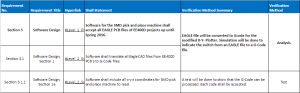
Software Design
Objective
To verify Software design, a test will be conducted to verify the process of converting an EAGLE file to GCode in order to send it to the modified Makeblock X-Y Plotter Robot Kit to move. The Z-axis software will be modified to control as if it was an X-axis and Y-axis.
Requirements
Section 3.1.1
Software shall include all x-, y-, and z-coordinates for SMD pick and place machine to read.
Applicable Tools
GRemote Graphic User Interface (GUI)
Notepad++ Application
| Equipment Type |
Name (Brand) |
Tolerance |
| Mitutoyo S/N 12519090 |
Caliper |
0.001” |
Procedure
A test for the X-axis and Y-axis motors have been conducted previously given an EAGLE file from G-Code.
https://www.arxterra.com/spring-2016-3d-smd-conversion-of-eagle-file-to-gcode-initial-process/
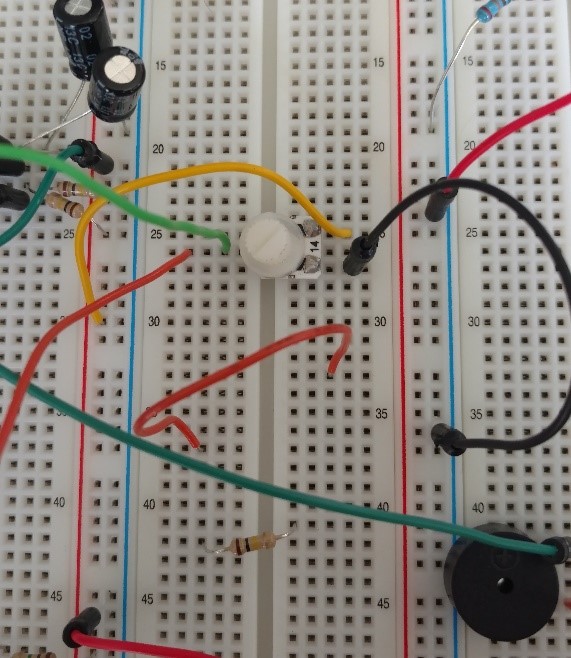
- Set-up Z-axis movement by attaching stepper motor to Z-axis structure.
- Connect stepper motor to Me Stepper Driver. Set switches to H H L (⅛ steps).
- Connect corresponding Me Stepper Driver to Port 10.
- Plug in Me UNO Shield and turn on switch to provide 12 V to stepper motor.
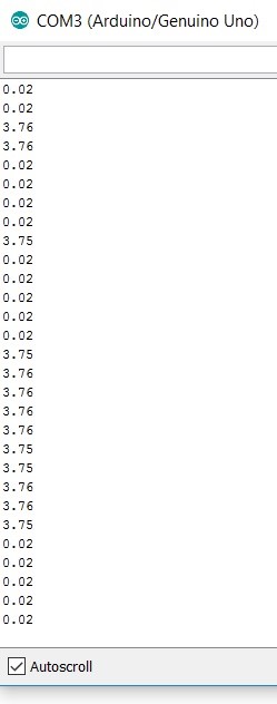
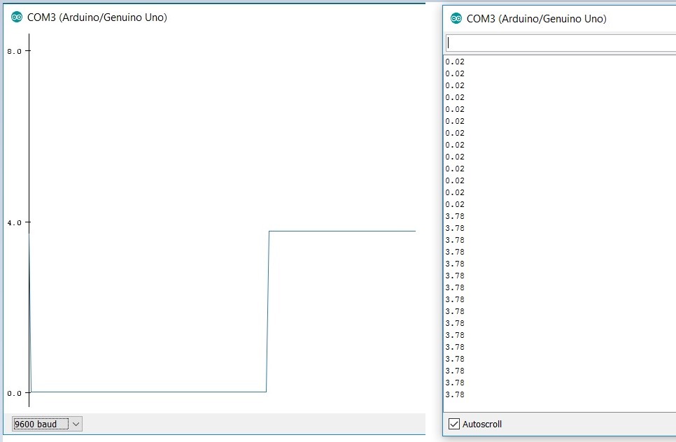
- Zero out Z-axis on GRemote GUI by entering “G92”.
- Measure initial height of Z-axis structure to the nearest 0.001 inches.
- On GRemote GUI, enter “Z100”.
- Wait until stepper motor stops running and measure the final height of the Z-axis structure to the nearest 0.001 inches.
“Z100” is a command that tells the Z-axis structure to move 100 mm when the Me Stepper driver is H H L. This procedure we will confirm the height difference of the Z-axis.
Reel Feeder Design
Objective
To verify the reel feeder design has the correct function, a test will be conducted to determine its parameters and design.
Requirements
Section 4
The SMD pick and place machine shall have four 8mm reel feeders and one IC tray.
Section 4.1
All SMT resistors and capacitors shall remain in cut-tape of the reel feeders until the vacuum nozzle is ready to pick up the component.
Section 4.1.1
All reel feeders shall be installed on the working area, 12.2”x15.35”(310mmx390mm).
Section 4.1.2
Bracket to hold cut-tape of the reel feeders shall be higher than 0.04″.
Section 4.1.3
All motors used to peel off cut-tape of reel feeders must rotate 360°.
Section 4.2
IC tray shall store all IC chips required for one PCB assembly.
Section 4.2.1
IC tray shall be installed within working area, 12.2”x15.35” (310mmx390mm).
Applicable Tools
Hardware:
Reel Feeder
Micro Servo FS-90
| Equipment Type |
Name (Brand) |
Tolerance |
| Mitutoyo S/N 12519090 |
Caliper |
0.001” |
Procedure
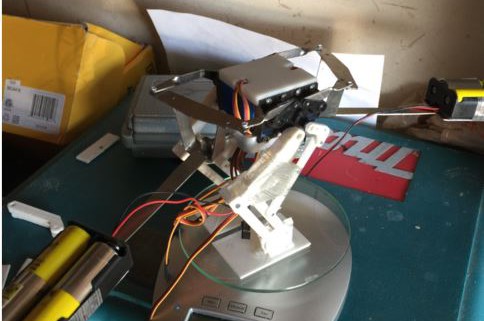
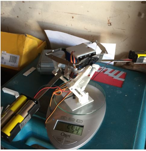
Note: Photos will be attached and documented
- Install reel feeder to the aluminum surface. Attache reel with SMT components.
- Install the IC tray to the working area.
- Install micro servo to reel feeder bracket. Servo wheel shaft shall be placed at an angle of approximately 45°. Record Servo wheel angle.
- Attach Z-axis and move the X-Y-axis motors to a component. Measure the clearance around the Z-axis. Record the clearance tolerance, which includes the distance around both the reel feeder and IC tray. Measure the height of the IC tray.
- Operate the micro servo by turning 360°. This requires timing of the speed of the micro servo and must be determined in the Arduino Code. Record this time.
- Determine initial measurement of the reel on the reel feeder. Record this measurement
- With the cut-tape attached to the micro servo wheel shaft, reel in the cut-tape. The SMT components counteract this force by moving back.
- Observe the elevation of the reel feeder. Record the height of the reel feeder.
- Record the distance of the SMT components traveled.
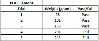
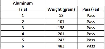
Results Template
| Angle of Servo Shaft |
Z-Axis Front (in.) |
Z-Axis Left side (in.) |
Z-Axis Right side (in.) |
Z-axis Height |
Vacuum Head Design
Vacuum Head Test
To verify the size of the vacuum nozzle design, a test will be conducted to determine that the size of the vacuum provides sufficient pressure to pick up an SMT component.
Requirements
Section 5 Vacuum Head Design
SMT component size 0402 shall be the smallest component that the pick and place SMD
machine can pick up.
Section 5.1
Vacuum system shall be able to pick up all SMT components as small as size 0402.
Section 5.1.1
Vacuum nozzle shall be smaller than 0.50 ± 0.05 mm.
Section 5.1.2
A solenoid valve for vacuum system shall keep a stable temperature under 160° F during Operation.
Section 6 Vacuum Head Design II
ATmega32u4 chip shall be the heaviest component that the pick and place SMD machine can pick up.
Section 6.1
Vacuum suction pad shall be smaller than 0.4″ ± 0.01″.
Applicable Tools
Procedure
- Determine actual mass of desired 0402 SMT component. Record under SMT component mass column.
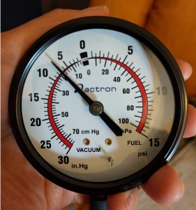
- With a T-bracket, measure the pressure by connecting both ends of the vacuum tubing and pressure gauge.
- Turn on vacuum pump and measure pressure. Record the value under pressure column.
- Calculate the minimum required diameter using the equation below.
- Measure the diameter of the vacuum nozzle being used. Using the equation below, plug in the diameter size and calculate the maximum mass allowed.
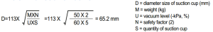
Equation 1. Obtained from (VMeca, n.d.).

Solenoid Valve Test
The purpose of this document is to verify that the solenoid valve can be used to control the the airflow of the vacuum system without overheating or damage to the vacuum tubing. Increased heat would affect the pressure within the tubing, thus could lead to errors in the operation of the pick and place machine.
References
Aquarium airline tubing is a Tuyau Standard type, which was found to operate at a temperature range of 86 ° F – 176° F (PennPlax, n.d. & Festo, 2016.)
Applicable Tools
Preliminary Calculations
We will estimate how many times the solenoid valve should close when placing one part. We would have to time when the solenoid valve should open and close.
- Close at PCB (discrepancy may be involved because the PCB locations vary, and the origin will be ignored because it will only be at the origin once. For the ease of this experiment, the opening and closing of the solenoid valve shall be at a minute by minute basis as shown in the calculations)
- Open at Reel Feeder
- Close back at PCB
Therefore, for one part to be placed, the solenoid valve must operate in 3 steps. The SMD pick and place machine estimates an assemble rate of 200 parts per hour.
200 parts/hour * 3 steps/part = 600 steps/hour
Convert to minutes:
600 steps/hour * 1 hour/ 60 minutes = 10 steps/minute
During our experiment, we will need to open and close the solenoid valve 10 times every minute.
Test Procedures & Criteria
- Connect the solenoid valve to operating voltage 12 Vdc. Solenoid valve should be open.
- Open and close the solenoid valve 10 times per minute for one hour.
- Every ten minutes, record the temperature of the barbed fitting hose. If the temperature goes higher than 176°F, turn off. (Tip: The temperature gun should record the temperature at the same area and distance to be consistent.)
- Measure and record the temperature of the solenoid valve to confirm that it is under 176°F +/- 10°F. under “Actual Final Temperature”.
- Cool the solenoid valve to room temperature and repeat one more time.
References
Atmel Corporation. (2016). ATmega16U4/ATmega32U4.
URL: http://www.atmel.com/images/atmel-7766-8-bit-avr-atmega16u4-32u4_summary.pdf
Festo. (2016). Plastic Tubing, Standard O.D.
URL: https://www.festo.com/cat/en-gb_gb/data/doc_ENGB/PDF/EN/OD-TUBING_EN.PDF
PennPlax, n.d. Aquarium Decorations Betta Accessories Maintenance.
URL: http://www.pennplax.com/pennplax%20pdf/Aquarium-Decorations-Betta-Accessories-Maintenance.pdf
Vmeca, n.d. How to select the proper vacuum pump.
URL: http://www.servikatalogen.no/Katalogdata/pdf/200802-1-2-3.pdf
Wikipedia. (2007). Image of a Cable with Seven Meter Radius.
URL: https://en.wikipedia.org/wiki/Bend_radius#/media/File:Bendradius.svg
Yadav, A. , Mehta, S. , Sawant, S. , Pujari, C. , & Chaudhary, M. (2014). Pick and place robotic
system for assembly of thermostat radiator valve.International Journal of Engineering
Trends and Technology, 11(3), 111-113.