Spring 2018 3DoT Hexy System Cable Tree

By: Raymundo Lopez-Santiago (Mission, System, and Test) & Kris Osuna (Electronic and Controls)

Verified by: Eduardo De La Cruz (Project Manager and Manufacturing Engineer)

Approved by: Miguel Garcia (Quality Assurance)

Table of Contents

Introduction

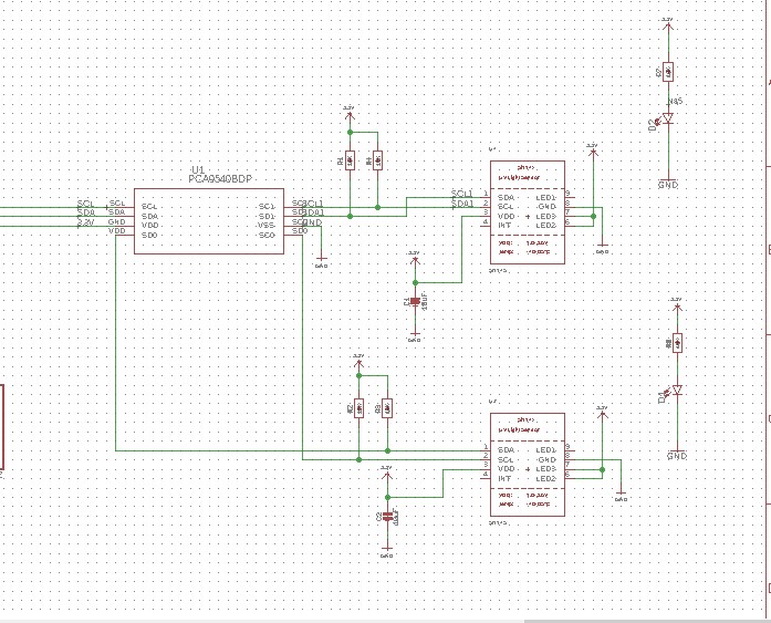
This blog post covers 3DoT Hexy’s cable tree design. 3DoT Hexy will use a total of 29 wires to connect to peripherals from the custom sensor PCB. The final cable tree design is shown in Fig. 1 (side view). The orange lines indicate the use of black spiral wrap protective sheathing which provides cable protection and flexible routing for all wires used. The rest of the wires (ribbon) are bundled according to their routing destination with black shrink tube. An example is packaging 4 wires (SDA, SCL, 3.3V, and GND) for each light sensor.  See Fig. 2 for a visual.

Update May 08, 2018

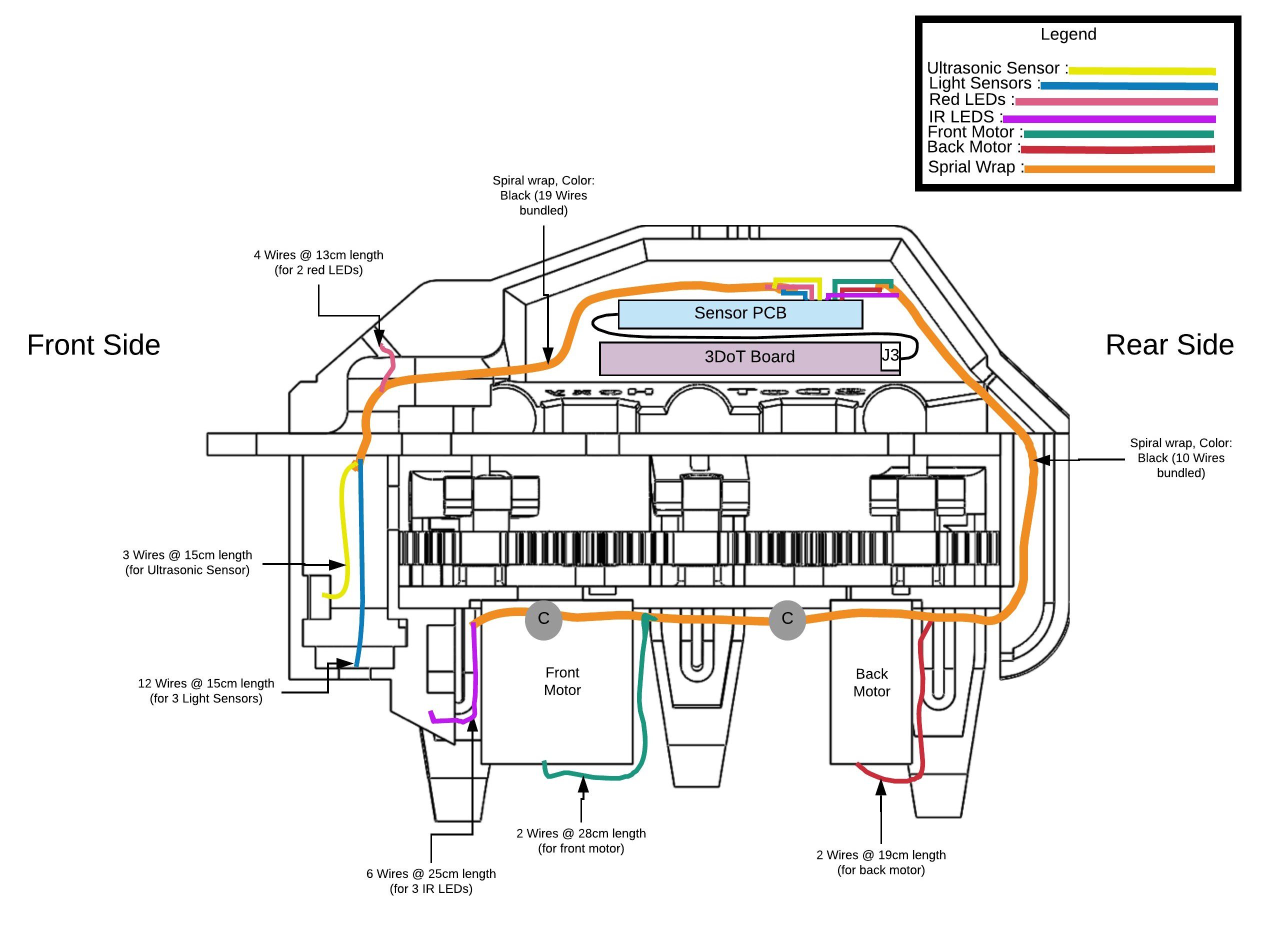
Fig. 1: Side view of 3DoT Hexy: Cable Tree (colored using Lucidchart)

Ten wires will be bundled inside spiral wrap and routed to the bottom part of the robot for the two micro metal motors and the three IR LEDs. Nineteen wires will be bundled inside spiral wrap and routed to the top part of the robot for two red LEDs, an ultrasonic sensor, and three light sensors. Wire clips will be used keep spiral wrap intact while routing wires for peripherals. This is represented as gray dots in Fig. 4.

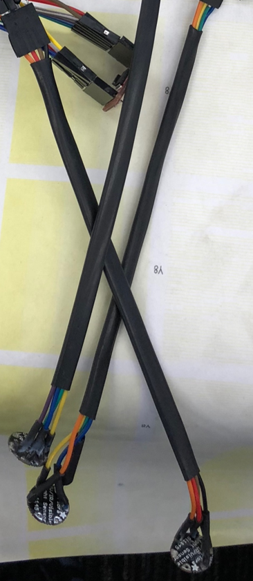
Fig. 2: Package of 4 wires (SDA, SCL, 3.3V, and GND) for each light sensor 


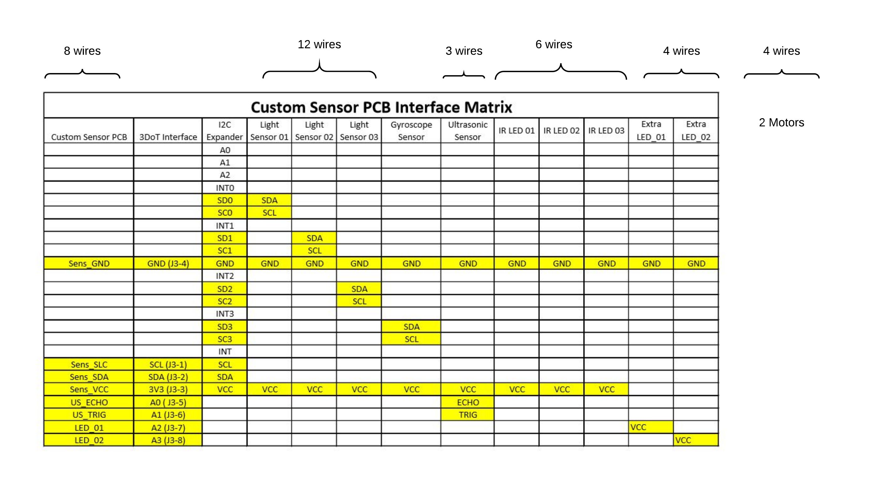
Fig. 3: Final decision on wire designation

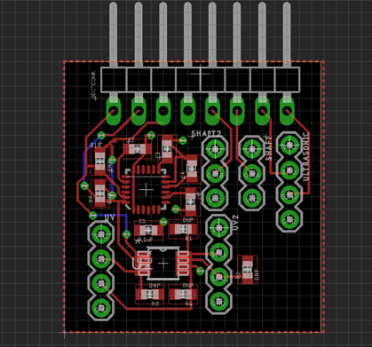
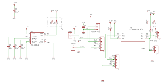
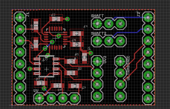
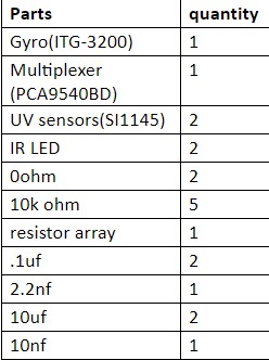
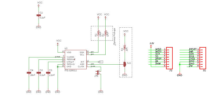
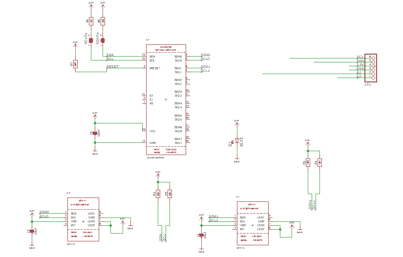
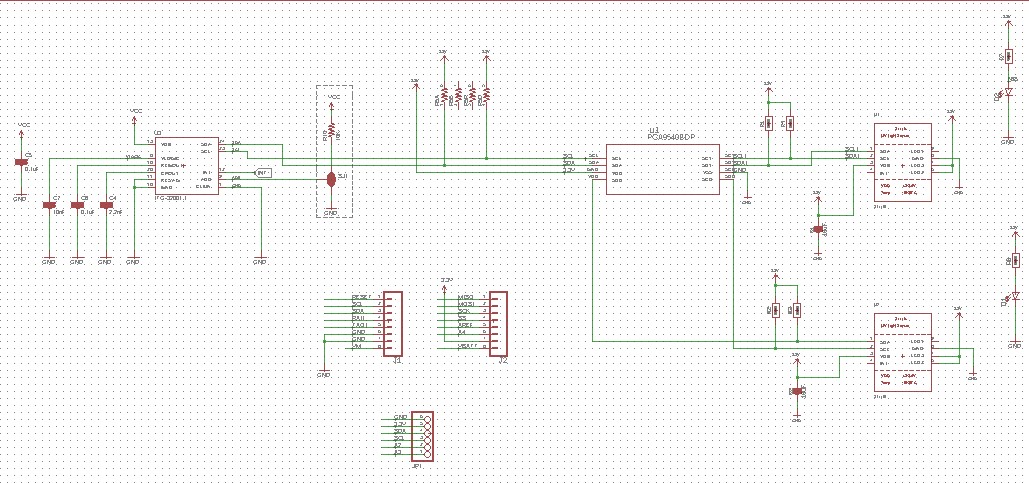
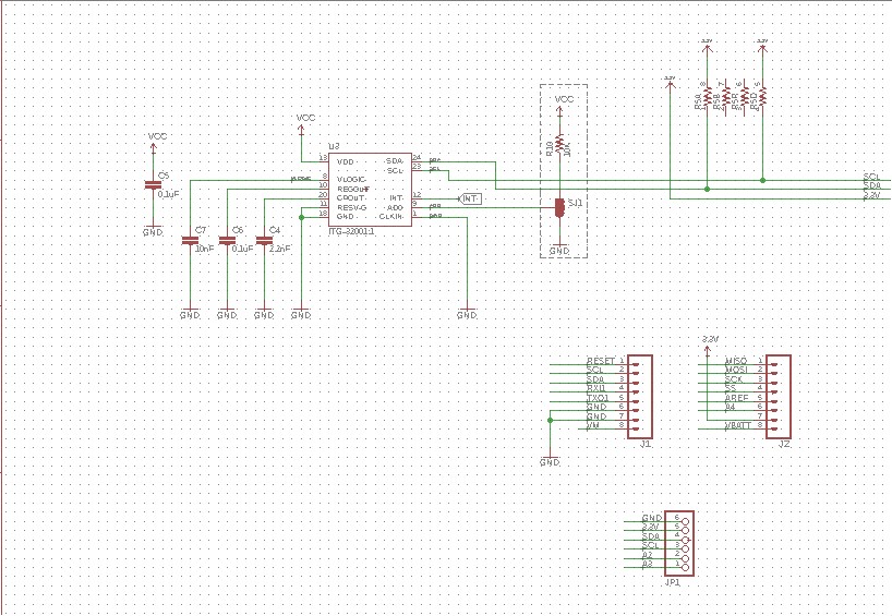
The 3DoT board will have female type connector (8 pins) to connect to the custom PCB sensor board’s 90-degree connector (8 pins). The gyroscope sensor and 4-channel I2C expander are integrated into the custom sensor PCB. The rest of the peripheral devices with information on length and number of wires used are as follows:


  • Adafruit Light Sensor Si1145 (x3) – 12 wires @ 15 cm length
  • Parallax Ping Ultrasonic Sensor (x1) – 3 wires @ 15 cm length
  • Red LEDs (x2) – 4 wires @ 13cm length
  • Micro Metal motor FIT0481(x2) – 4 wires @ 19 cm and 28 cm length
  • IR LEDs (x3) – 6 wires @ 25 cm length


In Fig. 4, the initial wire designation for each peripheral device used is shown. In that revision, a total of 26 wires was to be used. After exploring other design solutions, a final representation for 3DoT Hexy’s peripherals with the number of wires used can be seen in Fig. 1.


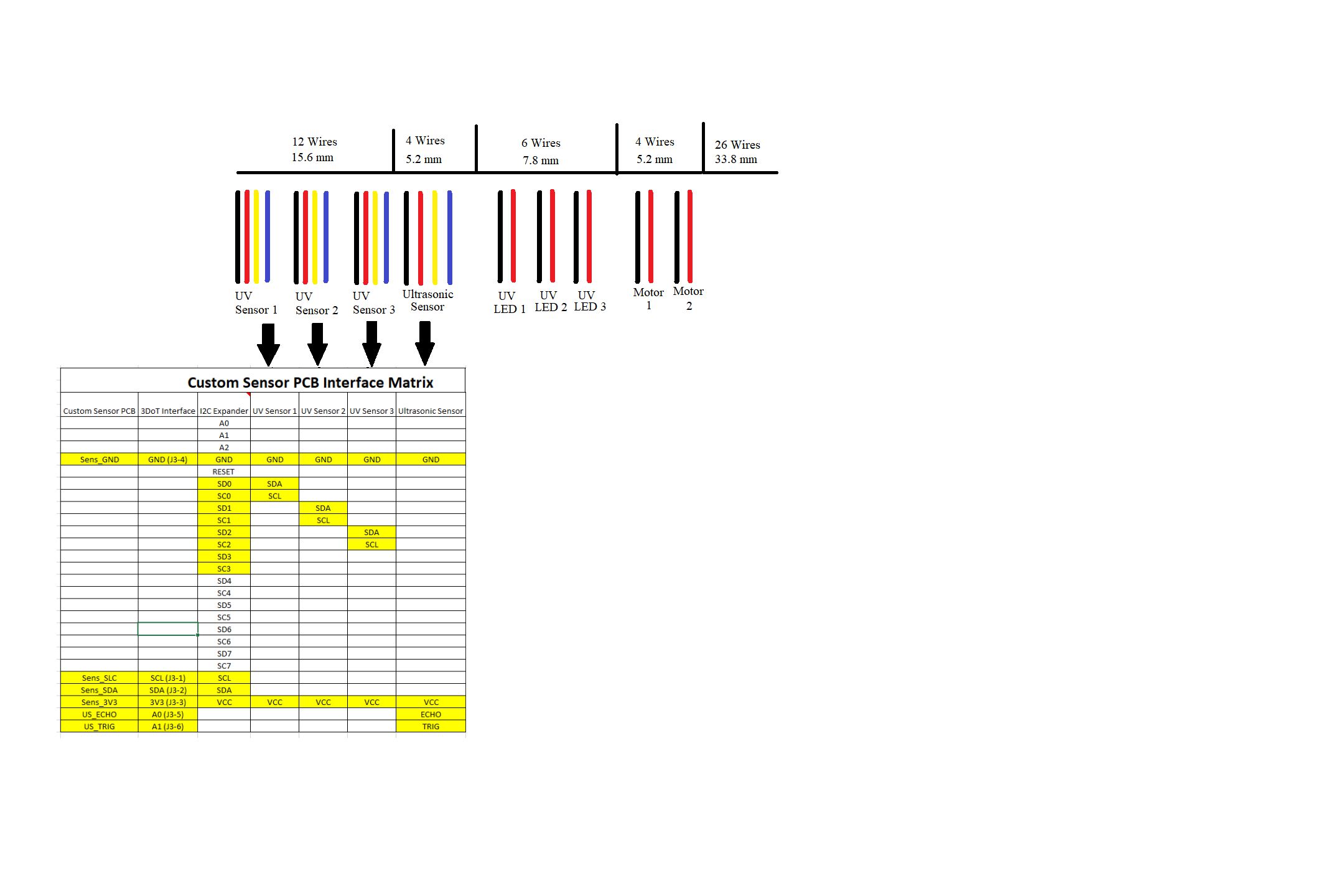
Fig. 4: Initial wire designation approach

Conclusion

Based on our design, it did require a lot wires which caused some issues when integrating all of them to their final position/destination. One main problem was with the positioning of the three-light sensors. A recommendation for a design improvement is to integrate the light sensors into the custom sensor PCB and place the PCB at bottom front bracket. The issue that needs to be further looked at is the 30-degree angle needed for the IR LEDs and the positioning so they maintain that angle. Another recommendation is start the design of the robot by first thinking about the wiring route and possibly integrating 3D printing wire assist clips to ease in the final product wiring.

References

  1. https://www.arxterra.com/spring-2018-3dot-hexy-3d-model/
  2. https://www.arxterra.com/spring-2018-3dot-hexy-system-block-diagram/
  3. https://www.arxterra.com/spring-2018-3dot-hexy-interface-matrix/

Spring 2018 AT-ST Gyro

By: Intiser Kabir (Project Manager) and Danny Pham (Manufacturing)

Approved By: Miguel Garcia (Quality Assurance)

Table of Contents

Introduction

Our research on the Gyro is to see if it is a good mechanism to help balance our AT-ST robot. We are 1st going to test how the Gyro calibrates when moved around. After that, we are going to see if the Gyro can help control the head and “tail” feature of our AT-ST robot, which are going to be used as a balancing mechanism. To do so, we are trying to see how Gyro can control Servos to give us an idea how to set up the Gyro-Servo balancing mechanism.

Materials

  • 1 x MPU-6050 (Gyro)
  • 1 x Arduino Uno
  • 1 x connection cord
  • 1 x Micro Servo
  • 4-7 x Wires
  • 1 x breadboard (however it might not be needed depending on the type of wires you use)

Testing the MPU6050

Fritzing Diagram

Figure 1: The circuit above is used to see calibration of the Gyro

Figure 2: The circuit above is where you control the servo arm with a Gyro

For our build since MPU6050 Wiring:

  • SCL – A5
  • SDA – A4
  • VCC – 3.3V
  • GND – GND
  • INT – PIN3
  • Servo Wiring:
  • VCC – 5V
  • GND – GND
  • Control – PIN3

Instruction

Gyro Calibrations:

  1. Connect the gyroscope to the Arduino using the fritzing diagram (Figure 1).
  2. Download the MPU6050 and I2Cdev libraries in the GitHub link in the references below.
  3. Copy the MPU6050 and I2Cdev folders into the Arduino libraries.
  4. Now open up the MPU6050_DMP6 file in Arduino under examples.
  5. Make sure the board and port are selected. Verify and upload the code to the Arduino.
  6. Open up the serial monitor and set the Baud rate to at least 15000.
  7. Follow the instructions. Enter a character and the coordinates will be given shortly.

Gyro – Servo Control:

Set up circuit like this: 

Figure 3: Physical Set Up

MPU6050 Wiring:

  • SCL – A5
  • SDA – A4
  • VCC – 3.3V
  • GND – GND
  • INT – PIN3

Servo Wiring:

  • VCC – 5V
  • GND – GND
  • Control – PIN3


  1. Download this Code: https://drive.google.com/file/d/0B0SU0douW9lVenJ0Vng0QlEyUDQ/view
  2. In order for the sketch to work you will need to install i2cdevlib library to Arduino library folder:https://github.com/jrowberg/i2cdevlib
  3. Bring the MPU close to servo
  4. Move MPU around to see the servo around moving around

Watch this video as reference: https://www.youtube.com/watch?v=vSKEH0FwhUE

Results

Figure 5: Output of the Calibration code

The calibration tells the x,y,z directions of the gyro.

Figure 6: servo arm moves at the same time as the gyro

It is sort of hard to tell from the picture, the servo arm moves depending on the change of position of the gyro just to be aligned with it.

Conclusion

From this research, we can see the Gyro can be useful in our balancing mechanism since we can control the directions the servos move. From the research, we can see how the Gyro can be calibrated when we move it around. We are planning to do more testing regarding our balancing mechanism for a future task using the Gyro.

Reference

  1. https://github.com/jrowberg/i2cdevlib
  2. https://www.youtube.com/watch?v=GjHxwDLBh00
  3. https://www.youtube.com/watch?v=vSKEH0FwhUE
  4. http://fritzing.org/projects/arduino-uno-gy-521
  5. https://maker.pro/arduino/tutorial/how-to-control-a-servo-with-an-arduino-and-mpu6050

Spring 2018 AT-ST Custom PCB Layout/Design

By: Shweta Hebbalkar (Electronics and Controls – Hardware)

Verified By: Intiser Kabir (Project Manager)

Approved By: Miguel Garcia (Quality Assurance)

Table of Contents

Introduction

For the AT-ST project, one of our goals is to create custom PCB using Eagle software. This software allows the user to generate PCB layouts, in order to use the Eagle software I need to learn how to use the software. With lack of experience using the Eagle software previously, it took me a week to two weeks to learn the general concept. So overview of the concepts is learning a PCB, also it is most common named “printed wiring board” or “printed wiring cards”. So it is a board that has lined and pads that connect various points together.

Transformation #1

The first thing I ever built in the Eagle CAD is the flowing figure, a schematic and PCB layout. In the figure one the schematic is for the op-amp amplifier I followed this schematic from the workshop that was directed by Chris and others.  Creating the PCB layout was easy to follow basically I moved all the components into the black box and then AutoRoute the trace.

Figure 1: Schematic

Figure 2: PCB #1

Figure 3: Frontside of PCB #2

In the picture above, there are traces that electrically connect the various connectors and component to each other. A PCB allows signals and power to be routed between physical devices.

Transformation #2

After two weeks of refining my skill in Eagle CAD with help of the Chris and others at the workshop. I was finally started designing my very first custom PCB layout schematic. When I was designing the circuit, it took me four days to find the library that I need it to create the custom PCB layout. Eventually, I was successful to get all the all the library that I need it, for example, the ultrasonic sensor the gyroscope and i2c expander as shown below in schematic and the board.

Figure 4: Iteration #2 schematic

In fig 4 the schematic was just placed on the template thinking that they will be all connecting in the board.

Figure 5: PCB layout

In Fig 5 the board layout, I placed all the components in the black box and then arranged in preferred to make it in compact space due to requirement. Afterward, I try to route the i2c expander with an ultrasonic sensor. In conclusion, from these we all understand that I need more practice then I thought and also need more clear instruction as well.

Transformation #3

In order to send in the custom PCB layout to print, I have to illustrate my board to get approval from our Customer. Which is very useful because professor Hill helped me the lot to make my board even more efficient. For example, the routing line has to be the 45-degree angle and it should be the clean line. If I am using polygon plane the top one supposed to be ground and the bottom one should the source. Always make sure to have the right parts if not then I redo the board design. According to the team consensus, we decide that we are going to make our PCB as the front shield.

Though this images below is my final version before getting approval. I had to go through many iterations. I had to connect all the lines in the schematic and I have to make it look easier to read for others.

Figure 6: New updated Schematic

Figure 7: Updated PCB

Unfortunately, we did not inform our professor that we are changing our custom PCB from top shield to the front shield. Still, the images above and I went with and I design our PCB.  Then After emailing professor this board to get approval from our professor however he emailed me back saying that why am I using the front shield. Then I respond to him saying that we need to use the analog pin, therefore, we are using the front shield. However, the professor said we don’t need to use analog pin we need digital pins and that pin is given in the top shield so I have to redo the custom PCB again.

In conclusion, we did not inform the customer beforehand with my design. Which means that I need I made myself double the work. The more time I spent with design PCB, I became more cautious because we would have to save time and print the board right away because printing board takes a lot of time.

Transformation #4

After getting some feedback from Customer, I already lost a big amount of time, which means that I get to have less time printing board, however, I started designing the top shield. With many changes like the routing and the get the right parts package size for schematic chaining any specifications according to professor liking I get approval the image below.

This is schematic is final schematic after many variations.

Figure 8: Finalized Schematic

The final PCB board that we send it to OSHPARK to print.

Figure 9: Finalized Custom PCB

Maintaining low expectation with my first board design because they had lots of problems and the final was my 25th board design that had the fewer error. The schematics are important and trying to design a board with a good schematic in place first is an exercise in futility.

In conclusion, I have learned lot more from Hill then division manager although they were helpful, mostly it is our job own responsibility to learn the eagle software.

Goliath Spring 2018 – Mock Up Motor Under Load

By: Ryan Nguyen (MST Engineer)

Verified By: Ernie Trujillo (Project Manager)

Approved By: Miguel Garcia (Quality Assurance)

Test Description

A mock-up motor under load test was performed to determine how much current the Goliath’s motors would draw while being put on mock loads, which were weights. Since the amp-meter has a large resistance, direct current measurement was not possible, as only a very small amount could flow through and the motors didn’t even turn. In place, a voltage measurement was taken over a 100-ohm resistor to determine the current of the motors. The motors would lift the weight, hung on a gear, and the highest voltage is recorded. Testing stopped when the weight reached 80 grams, any more than that the motors would not move. 80 grams per motor is quite good as the Goliath robot would probably weigh between 150 – 200 grams. The test also suggested that the maximum current pull from motors are about 35 mA each, which is useful for the power budget.

Figure 1 – Table displaying voltage and current values of both motors at varying loads.

Resources


Goliath Spring 2018 – Custom Shield Layout

By: Milton Ramirez (E&C Engineer)

Verified By: Ernie Trujillo (Project Manager)

Approved By: Miguel Garcia (Quality Assurance)

Table of Contents

Introduction

This blog post will go over all the different iterations for the PCB layout for Goliath.

Eagle Layouts

Figure 1. Layout for the Gyro PCB

This design was just a rework of the ITG-2200 breakout, to fit on top of the 3DoT board. All the capacitors and resistors are connected to ground and are paired together so that it could look nice. Same goes for all of the capacitors and resistors connected to voltage source 3.3V. This layout is also using an old set of pins that have SCL on the right side of the connectors and SDA on the left side. The top layer is connected to ground while the bottom layer is connected to 3.3V

Figure 2. UV Sensor board.

This board connects two UV sensors to a multiplexer, which connects to the SDA and SCL of the 3Dot board. The multiplexer is on the bottom layer of the board. This was done to make space on the top layer. All the resistors that were connected to their respective part were placed together. For example, resistors R1, R4, and capacitor C1 are placed next to U4. The six pins were placed on top so they can connect to the six pins on the bottom of the 3dot. This was an earlier design of the 3dot since the new 3dot has 8 pins now. Same as the gyro, which the top layer is connected to ground and bottom is connected to 3.3V.

Figure 3. The final board design for the Goliath PCB.

The final layout combines the previous two layouts. In this layout, the connectors on top are for the path-finder breakout board. The connectors on the side are the so that our PCB can be mounted on top of the 3dot board. The UV sensors are spaced at 1.7cm. The LEDs are both placed under the UV sensors so that the best possible readings from the UV sensors can be obtained. The capacitors C1, C2, and C5 are all coupling capacitors and are placed as close as possible to the voltage pins of the two UVs and Gyro. The I2C expander from the previous design was replaced with the 2 address I2C multiplexer PCA9540BDP. The pull-up resistors, the range-finder connectors, Gyro and I2C share were replaced with a resistor array to make more space on the top left side. This helped because the SDA and SCL pins are on the top left side and needed as much space as possible since the I2C, Gyro, and range-finder are all connected to those same pins. The top layer of the PCB is grounded while the bottom layer is connected to the voltage source 3.3V.


These next two figures are earlier designs of the final design since this is the version that went through many iterations.

Figure 4. The first iteration of the final PCB.

This circuit used an 8 address multiplexer and had a set of pull-up resistors for both the multiplexer and gyro. The coupling capacitors are also not where they’re supposed to be. Also, this design was still using the 8 address I2C. Since this chip was big, it was placed in the bottom layer to make space for the rest of the parts. The LED’s are also missing in this iteration.

Figure 5. Another iteration that was closer to the final design. One notable difference from this design is that I tried to use connectors for the LEDs. This iteration has the 2 address I2C and the resistor array added.

Parts Required

Figure 4. Final Parts list for the PCB

Conclusion

The PCB was approved April 21, 2018. Was ordered on April 26, 2018, and will arrive May 5, 2018.

References

  1. https://www.sparkfun.com/products/11977
  2. https://www.digikey.com/product-detail/en/nxp-usa-inc/PCA9540BD118/568-1844-1-ND/789976
  3. https://www.adafruit.com/product/1981
  4. https://www.adafruit.com/product/2717?gclid=CjwKCAjwlcXXBRBhEiwApfHGTd0vBvwKsP8KS7RMRyuV4j720AR6SxzWgmhaRgt9JazlS-hEpLF4HhoCSbQQAvD_BwE

Goliath Spring 2018 – System Schematics

Written by Milton Ramirez (E&C PCB Engineer)

Verified by Ernie Trujillo (Project Manager)

Approved by Miguel Garcia (Quality Assurance)

Table of Contents

Introduction

These are the schematics from the multiple PCB boards that were designed for the Goliath. The PCB schematics consisted of a gyro shield, a UV shield, and the final design which combined the previous two designs.

Schematics

Figure 1. Gyro Shield Schematic

This schematic is an exact copy of the ITG-2200 breakout board schematic. The only difference is the two 8 pin connectors. This was done so that it can go mounted on top of the 3dot board. The gyro connects to the SDA and SCL pins in the connectors.

Figure 2. UV Sensor Shield Schematic

This schematic has a 6 pin connector that the I2C expander connects through the SDA And SCL pins. The first UV sensor is connected to the SCA0 and SCL0 pins in the I2C expander, and for the other UV sensor, the SDA, SCL, SDA1, SCL1, SDA0, and SCL0 pins have pull-up resistors. Finally, there is one LED to find the UV sensors to read the lines in the maze.

Figure 3. Final PCB Schematic

Figure 4. Close-up of the left side of the schematic for the final PCB.

Figure 5. Close-up of the right side of the schematic for the final PCB.

Conclusion

In the end, we scrapped the last two designs and combined them into one PCB. This PCB connects SDA and SCL to the I2C expander and the gyro sensor.  This time we added connectors on the board for range-finder which also connects to SDA and SCL pins. Since all three of these are connected to the same SDA and SCL, there is only one pair of pull up resistor for all three parts. This pull-up resistor was also replaced with a resistor array. The I2C expander was changed from 8 addresses to 2 addresses since we only need two for the UV sensors. The gyro lost the jumper, which was designed just in case we needed to connect an external clock. Two LEDs were added since it makes it easier for the UV sensors to read the line if each sensor has its own LED.

References

  1. https://www.sparkfun.com/products/11977
  2. https://www.digikey.com/product-detail/en/nxp-usa-inc/PCA9540BD118/568-1844-1-ND/789976
  3. https://www.adafruit.com/product/1981
  4. https://www.adafruit.com/product/2717?gclid=CjwKCAjwlcXXBRBhEiwApfHGTd0vBvwKsP8KS7RMRyuV4j720AR6SxzWgmhaRgt9JazlS-hEpLF4HhoCSbQQAvD_BwE

Spring 2018 AT-ST Work Breakdown Structure (WBS)

By: Intiser Kabir (Project Manager)

Approved By: Miguel Garcia (Quality Assurance)

Table of Contents

Introduction

The idea of the WBS is to breakdown who does what for the project. The Project Manager assigns all tasks to the group and divides the work into who is the best fit for the job as well list out the tasks from the task matrix. WBS looks like a flowchart that shows where each specific task goes to per division.

WBS

Figure 1 Workbreak down structure

Description

The idea of the WBS is the breakdown who does what for the project based on the task matrix and job description. It is broken down to each division the task belongs to. Some people within groups also volunteer to task outside of their specialty or working with others. So the breakdown is structured around this. This WBS will be used to help create PBS.

References

  1. https://docs.google.com/spreadsheets/d/1hYPJQWkk-FtJcmEzwJh0wv_LhTuU2_OUg5NqZrFQ7T0/edit#gid=1180904142
  2. http://web.csulb.edu/~hill/ee400d/Lectures/Week%2001%20Company%20and%20Mission/d_Job%20Application.pdf
  3. http://web.csulb.edu/~hill/ee400d/Lectures/Week%2001%20Company%20and%20Mission/c_Job%20Descriptions.pdf

Solar Panel Charging

By: Mohammad Yakoub (Mission, Systems, and Testing)

Verified By: Jordan Smallwood (Project Manager)

Approved By: Miguel Garcia (Quality Assurance)

Table of Contents


Introduction

The objective of this blog post to find a way to charge the main battery with the solar panel cells. There are different ways to go about this, but I found that the best way for our project is to use a charge controller. This way we can make sure that we do not overcharge the battery with our solar panel.

The specific charger we are using is called The xcsource Solar charge Controller. This specific one is purchased from amazon.

Figure 1: Top View of Charge Controller

A charge controller is basically a voltage/current regulator to keep batteries from overcharging. It regulates the voltage and current coming from the solar panel going to the battery. Most solar Panels supply more voltage than rated, because these panels need ideal conditions to be able to provide full power, and those conditions are impossible to meet. The panels are designed to provide power than rated, so it can still function in less than ideal conditions. So without regulating the solar panel The battery can be damaged from overcharging.


How it Works

The way that works is we connect the solar panel and the battery to the charge controller. The charge controller will charge the battery and power our components. The charge controller will charge the battery until the it reaches a full charge and as the battery charge gets higher the controller will reduce the solar panel output to avoid overcharging the batteries. Once the battery is nearly full, the charge controller only sends a trickle charge to top off the batteries without overcharging them. This process is known as the off grid charging. An alternative process is to allow the solar panel to supply power to our components directly, but that is not as efficient, and will not be able to supply enough energy for the motors. When the battery reaches a full charge the controller will switch the power output of the solar panels to a dedicated load, such as a light or heating filament.

Figure 2: Typical connection of Solar Panel – Battery Controller


Conclusion

As mentioned earlier the charge controller is mainly used to prevent overcharge, and improving charge quality. But that is not the only advantage of using the charge controller, it can also prevent battery discharge in low or no-light conditions. Discharging can happen when the sunlight goes out the battery will discharge to heat the solar panels. However, the charge controller will detect the batteries discharging and disconnect the panels, to prevent the discharging of the battery. This can also be achieved by using solar panels with blocking diodes that prevent battery discharge during low or no-light conditions, but such systems are not as efficient when using high power solar panels.


References

  1. https://www.batterystuff.com/kb/articles/solar-articles/solar-info.html
  2.  https://www.amazon.com/Controller-Charge-Battery-Regulator-Protection/dp/B010FNO9NU/ref=sr_1_3?ie=UTF8&qid=1525723142&sr=8-3&keywords=solar+controller+10a
  3. https://www.aliexpress.com/item/10A-CMP12-12V-24V-intelligence-Solar-cells-Panel-Battery-Charge-Controller-Regulators/619325690.html?src=google&albslr=119861048&isdl=y&aff_short_key=UneMJZVf&source=%7Bifdyn:dyn%7D%7Bifpla:pla%7D%7Bifdbm:DBM&albch=DID%7D&src=google&albch=shopping&acnt=708-803-3821&isdl=y&albcp=653153647&albag=34728528644&slnk=&trgt=61865531738&plac=&crea=en619325690&netw=s&device=c&mtctp=&aff_platform=google&gclid=Cj0KCQjwodrXBRCzARIsAIU59TK4xse4VJUY-AmA0KTMhI5Mr_pqDeCrQ-Z9OL_oY1lKCcZHztYFMXEaAlqtEALw_wcB&gclsrc=aw.ds
  4. http://uisalumnisage.org/solar-light-wiring-diagram-2/for-solar-light-wiring-diagram/

Stepper Motor Study

By: Adolfo Jimenez (Manufacturing)

Verified By: Jordan Smallwood (Project Manager)

Approved By: Miguel Garcia (Quality Assurance)

Table of Contents


Introduction

In order to test the articulation of the solar panels before they were assembled onto the chassis an EasyDriver stepper motor driver was used to run and test the motors, and thus by extension the solar panels. Stepper motors can move an exact amount of degrees (or steps) when programmed to do so. This gives us total control over the motor, allowing us to move it to an exact location and hold that position. This is done by alternating power sent to 2 separate coils inside the motor at fractions of a second. A stepper motor combined with a motor driver and microcontroller allows us to dictate the speed and amount of steps taken in any direction making them ideal for our solar panel articulation system.


Parts Used

  • Bipolar Stepper Motor (ROB-09238)
  • EasyDriver – Stepper Motor Driver (ROB-12779)
  • Arduino UNO
  • Breadboard, Wires, 10k Resistor (x2), 12V Power supply

Figure 1: Typical Stepper Motor

Figure 2: Sparkfun Easy Driver


Assembly

First, the board needed to be assembled, that was a quick and easy job requiring the soldering of the 17 included header pins onto the board. The next step was wiring the entire setup, to do this we first needed to identify which of the four wires pertained to each coil wire pair within the motor. Looking at the datasheet for this stepper motor we can see that the red and green wires form one coil, while the yellow and blue form another. To test this, an LED can be connected to a wire pair on each lead. If the LED blinks while manually turning the motor shaft then those two cables indeed form a coil. The first coil pair should be plugged into Coil A+ and Coil A-, while the second coil pair plugs into Coil B+ and Coil B-. After further research it was discovered that there is no polarity on the coils, so you need not worry about plugging in a coil backwards onto the board. As per the specifications on the datasheet for the motor, a 12-volt power supply was selected to power the motor. All remaining connections can be seen in the following fritzing diagram:

Figure 3: Fritzing Diagram for Simple Stepper Motor Operation


Code

With the physical circuit built the following code was uploaded onto the Arduino UNO to begin controlling the motor. When the code is running, it waits for a button press (a LOW on Arduino pin 2 or 3) and then begins to rotate the stepper motor for the programmed number of steps. A push button switch was added between Pins 2, 3, and ground, with an accompanying 10K pull up resistor used for each pin at 3.3V. For this set up, pin 3 associated with the button on the left (LOW on pin 3) turned the motor clock wise, the button on the right (LOW on pin 2) rotated the motor counter-clockwise.

Figure 4: Code for Simple Operation of Stepper Motors


Conclusion

Utilizing this described setup I was able to test the stepper motors and begin working on the solar panel articulation for our rover. Messing with the code I found that using the motor at slower speeds appeared to provide me with more torque as spinning it at a slower RPM provided the greatest resistance against pressure applied on the shaft by squeezing it with my fingers. One thing to really note is the current adjustment potentiometer on the EasyDriver. I recommend that while the code is running, with a small screw driver slowly turn the potentiometer one way or the other. Depending on the type of motor you use (mainly its coil resistance) you may notice a difference as different current values might operate the motor much more smoothly than others.


References

  1. https://www.sparkfun.com/datasheets/Robotics/SM-42BYG011-25.pdf
  2. http://www.schmalzhaus.com/EasyDriver/Examples/EasyDriverExamples.html
  3. https://www.sparkfun.com/tutorials/400
  4. https://learn.sparkfun.com/tutorials/easy-driver-hook-up-guide?_ga=2.95969304.586601746.1525205163-1420080731.1522797085

Top 10 Blog Post Mistakes

The top mistakes that are seen year after year, that you must avoid!